- 您现在的位置:买卖IC网 > PDF目录5730 > AD8222HACPZ-WP (Analog Devices Inc)IC AMP INST DUAL PREC LN 16LFCSP PDF资料下载
参数资料
| 型号: | AD8222HACPZ-WP |
| 厂商: | Analog Devices Inc |
| 文件页数: | 8/24页 |
| 文件大小: | 0K |
| 描述: | IC AMP INST DUAL PREC LN 16LFCSP |
| 标准包装: | 64 |
| 放大器类型: | 仪表 |
| 电路数: | 2 |
| 转换速率: | 2 V/µs |
| -3db带宽: | 1.2MHz |
| 电流 - 输入偏压: | 500pA |
| 电压 - 输入偏移: | 120µV |
| 电流 - 电源: | 900µA |
| 电流 - 输出 / 通道: | 18mA |
| 电压 - 电源,单路/双路(±): | 4.6 V ~ 36 V,±2.3 V ~ 18 V |
| 工作温度: | -40°C ~ 85°C |
| 安装类型: | 表面贴装 |
| 封装/外壳: | 16-VQFN,CSP |
| 供应商设备封装: | 16-LFCSP(4x4) |
| 包装: | 托盘 - 晶粒 |
AD8222
Rev. A | Page 16 of 24
REFERENCE TERMINAL
The output voltage of an AD8222 channel is developed with
respect to the potential on the corresponding reference terminal.
Typically the reference terminal is connected to ground, but it
can also be driven with a voltage to offset the output signal. For
example, connect a voltage to the reference terminal to level-
shift the output so that the AD8222 can drive a single-supply
ADC. Both REF1 and REF2 are protected with ESD diodes and
should not exceed either +VS or VS by more than 0.3 V.
For best performance, source impedance to a reference terminal
should be kept below 1 Ω. As shown in Figure 44, the reference
terminal is at one end of a 10 kΩ resistor. Additional impedance
at the reference terminal adds to this 10 kΩ resistor and results
in amplification of the signal connected to the positive input.
The amplification from the additional RREF can be computed by
REF
R
kΩ
20
kΩ
10
2
Only the positive signal path is amplified; the negative path is
unaffected. This uneven amplification degrades the amplifier’s
CMRR.
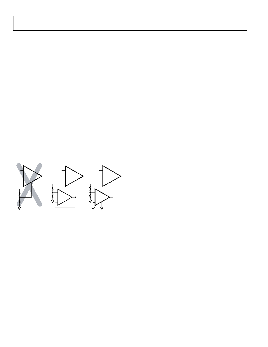
INCORRECT
AD8222
V
CORRECT
AD8222
OP2177
+
–
V
05
94
7-
05
4
CORRECT
AD8222
+
–
V
REF
Figure 45. Driving the Reference Pin
PACKAGE CONSIDERATIONS
The AD8222 comes in a 4 mm × 4 mm LFCSP. Beware of
blindly copying the footprint from another 4 mm × 4 mm
LFCSP part; the landing pattern may be different. Refer to
the Outline Dimensions section to verify that the PCB symbol
has the correct dimensions.
The AD8222 comes in two package varieties, both with and
without a thermal pad.
Package Without Thermal Pad
The AD8222 ships with a package that does not include a thermal
pad; it is the preferred package for the AD8222. Unlike chip
scale packages where the pad limits routing capability, the AD8222
package allows routes and vias directly underneath the chip, so
that the full space savings of the small LFCSP can be realized.
Although the package has no metal in the center of the part, the
manufacturing process does leave a very small section of exposed
metal at each of the package corners, shown in Figure 55 in the
Outline Dimensions section. This metal is connected to VS
through the part. Because of a possibility of a short, vias should
not be placed underneath this exposed metal.
Package with Thermal Pad
This package is included primarily for legacy reasons. Because
the AD8222 dissipates so little power, there is little need for the
thermal pad.
The thermal pad is connected internally to VS. The pad can
either be left unsoldered, soldered to an otherwise unconnected
PCB landing, or soldered to a landing connected to the negative
supply rail (VS). If pin compatibility with the AD8224 is
desired, the pad should not be electrically connected to any net,
including VS.
The solder process can leave flux and other contaminants on
the board. When these contaminants are between the AD8222
leads and thermal pad, they can create leakage paths that are
larger than the AD8222’s bias currents. A thorough washing
process removes these contaminants and restores the AD8222’s
excellent bias current performance.
LAYOUT
The AD8222 is a high precision device. To ensure optimum
performance at the PC board level, care must be taken in the
design of the board layout. The AD8222 pinout is arranged in a
logical manner to aid in this task.
Common-Mode Rejection Over Frequency
The AD8222 has a higher CMRR over frequency than typical
in-amps, which gives it greater immunity to disturbances, such
as line noise and its associated harmonics. A well-implemented
layout is required to maintain this high performance. Input
source impedances should be matched closely. Source resistance
should be placed close to the inputs so that it interacts with as
little parasitic capacitance as possible.
Parasitics at the RGx pins can also affect CMRR over frequency.
The PCB should be laid out so that the parasitic capacitances at
each pin match. Traces from the gain setting resistor to the RGx
pins should be kept short to minimize parasitic inductance.
Reference
Errors introduced at the reference terminal feed directly to the
output. Care should be taken to tie REF to the appropriate local
ground.
Power Supplies
A stable dc voltage should be used to power the instrumentation
amplifier. Noise on the supply pins can adversely affect
performance.
The AD8222 has two positive supply pins (Pin 5 and Pin 16)
and two negative supply pins (Pin 8 and Pin 13). Although the
part functions with only one pin from each supply pair connected,
相关PDF资料 |
PDF描述 |
|---|---|
| 68481-210HLF | BERGSTIK II .100" DR STRAIGHT |
| LT1210CR#TR | IC AMP CURR FEEDBACK 1.1A 7DD |
| N2520-50K2-RB | CONN HEADER 20POS R/A GOLD T/H |
| 3314-6602UG | CONN HEADER 14POS STR LONG LATCH |
| LT1207CS#PBF | IC CURRNT FEEDBK AMP DUAL 16SOIC |
相关代理商/技术参数 |
参数描述 |
|---|---|
| AD8222HBCPZ-R7 | 功能描述:IC AMP INST DUAL PREC LN 16LFCSP RoHS:是 类别:集成电路 (IC) >> Linear - Amplifiers - Instrumentation 系列:- 标准包装:50 系列:- 放大器类型:J-FET 电路数:2 输出类型:- 转换速率:3.5 V/µs 增益带宽积:1MHz -3db带宽:- 电流 - 输入偏压:30pA 电压 - 输入偏移:2000µV 电流 - 电源:200µA 电流 - 输出 / 通道:- 电压 - 电源,单路/双路(±):7 V ~ 36 V,±3.5 V ~ 18 V 工作温度:0°C ~ 70°C 安装类型:通孔 封装/外壳:8-DIP(0.300",7.62mm) 供应商设备封装:8-PDIP 包装:管件 |
| AD8222HBCPZ-RL | 功能描述:IC AMP INST DUAL PREC LN 16LFCSP RoHS:是 类别:集成电路 (IC) >> Linear - Amplifiers - Instrumentation 系列:- 标准包装:50 系列:- 放大器类型:J-FET 电路数:2 输出类型:- 转换速率:3.5 V/µs 增益带宽积:1MHz -3db带宽:- 电流 - 输入偏压:30pA 电压 - 输入偏移:2000µV 电流 - 电源:200µA 电流 - 输出 / 通道:- 电压 - 电源,单路/双路(±):7 V ~ 36 V,±3.5 V ~ 18 V 工作温度:0°C ~ 70°C 安装类型:通孔 封装/外壳:8-DIP(0.300",7.62mm) 供应商设备封装:8-PDIP 包装:管件 |
| AD8222HBCPZ-WP | 功能描述:IC AMP INST DUAL PREC LN 16LFCSP RoHS:是 类别:集成电路 (IC) >> Linear - Amplifiers - Instrumentation 系列:- 标准包装:2,500 系列:Excalibur™ 放大器类型:J-FET 电路数:1 输出类型:- 转换速率:45 V/µs 增益带宽积:10MHz -3db带宽:- 电流 - 输入偏压:20pA 电压 - 输入偏移:490µV 电流 - 电源:1.7mA 电流 - 输出 / 通道:48mA 电压 - 电源,单路/双路(±):4.5 V ~ 38 V,±2.25 V ~ 19 V 工作温度:-40°C ~ 85°C 安装类型:表面贴装 封装/外壳:8-SOIC(0.154",3.90mm 宽) 供应商设备封装:8-SOIC 包装:带卷 (TR) |
| AD8223 | 制造商:AD 制造商全称:Analog Devices 功能描述:Single Supply, Rail-to-Rail, Low Cost Instrumentation Amplifier |
| AD8223AR | 功能描述:IC AMP INST R-R LP 8SOIC RoHS:否 类别:集成电路 (IC) >> Linear - Amplifiers - Instrumentation 系列:- 标准包装:50 系列:LinCMOS™ 放大器类型:通用 电路数:4 输出类型:- 转换速率:0.05 V/µs 增益带宽积:110kHz -3db带宽:- 电流 - 输入偏压:0.7pA 电压 - 输入偏移:210µV 电流 - 电源:57µA 电流 - 输出 / 通道:30mA 电压 - 电源,单路/双路(±):3 V ~ 16 V,±1.5 V ~ 8 V 工作温度:-40°C ~ 85°C 安装类型:表面贴装 封装/外壳:14-SOIC(0.154",3.90mm 宽) 供应商设备封装:14-SOIC 包装:管件 产品目录页面:865 (CN2011-ZH PDF) 其它名称:296-1834296-1834-5 |
发布紧急采购,3分钟左右您将得到回复。