- 您现在的位置:买卖IC网 > PDF目录2137 > AD8231WACPZ-RL (Analog Devices Inc)IC AMP INST RRO 2.7MHZ 16LFCSP PDF资料下载
参数资料
| 型号: | AD8231WACPZ-RL |
| 厂商: | Analog Devices Inc |
| 文件页数: | 14/24页 |
| 文件大小: | 0K |
| 描述: | IC AMP INST RRO 2.7MHZ 16LFCSP |
| 标准包装: | 5,000 |
| 放大器类型: | 仪表 |
| 电路数: | 2 |
| 输出类型: | 满摆幅 |
| 转换速率: | 1.1 V/µs |
| 增益带宽积: | 7MHz |
| 电流 - 输入偏压: | 250pA |
| 电压 - 输入偏移: | 4µV |
| 电流 - 电源: | 4mA |
| 电流 - 输出 / 通道: | 70mA |
| 电压 - 电源,单路/双路(±): | 3 V ~ 6 V,±1.5 V ~ 3 V |
| 工作温度: | -40°C ~ 125°C |
| 安装类型: | 表面贴装 |
| 封装/外壳: | 16-VQFN 裸露焊盘,CSP |
| 供应商设备封装: | 16-LFCSP-VQ EP(4x4) |
| 包装: | 带卷 (TR) |
AD8231
Rev. B | Page 21 of 24
APPLICATIONS INFORMATION
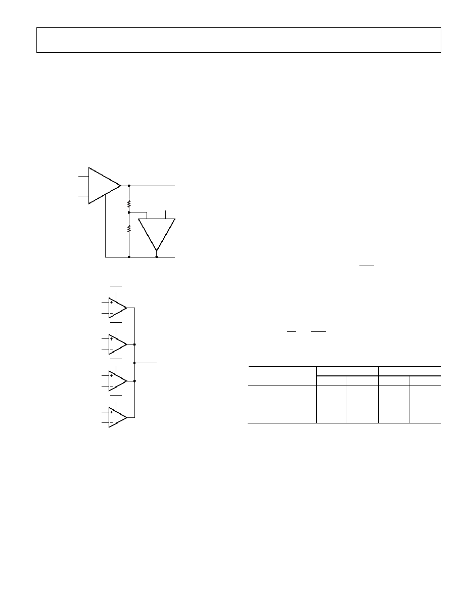
DIFFERENTIAL OUTPUT
Figure 53 shows how to create a differential output in-amp
using the AD8231 uncommitted op amp. Because this
configuration makes use of the reference terminal of the
in-amp, errors from the op amp and resistor mismatch result in
common-mode errors, rather than differential errors. Because
common-mode errors are typically rejected by the next device
in the signal chain, this circuit configuration adds almost no
extra error.
+IN
–IN
IN-AMP
VREF
4.99k
+
–
OP AMP
+OUT
–OUT
4.99k
REF
9
10
76
8
3
2
06
58
6-
03
5
Figure 53. Differential Output Using Operational Amplifier
MULTIPLEXING
SDN0
SDN1
SDN2
SDN3
06
58
6-
0
36
Figure 54. Four AD8231s in Multiplexing Configuration
The outputs of both the AD8231 in-amp and op amp are high
impedance in the shutdown state. This feature allows several
AD8231s to be multiplexed together without any external
switches. Figure 54 shows an example of such a configuration.
All the outputs are connected together and only one amplifier is
turned on at a time. This feature is analogous to the high-Z
mode of the digital tristate logic.
The resistors in the AD8231 instrumentation amplifier create a
resistive path from the output to the reference pin of about
100 kΩ. If a higher output impedance in shutdown mode is
desired, the reference pin can be driven with the op amp of
the AD8231. In this configuration, the output impedance in
shutdown is several GΩ, and many thousand AD8231s can
theoretically be multiplexed in such a way.
The AD8231 can enter and leave shutdown mode very quickly.
However, when the amplifier wakes up and reconnects its input
circuitry, the voltage at its internal input nodes changes dramati-
cally. It takes time for the output of the amplifier to settle. Refer
for different gains. This settling time limits how quickly the
AD8231 can be multiplexed with the SDN pin.
USING THE AD8231 WITH BIPOLAR SUPPLIES
The AD8231 can be used with bipolar supplies as long as the
maximum voltage drop between the supply rails is kept below
6 V and all input voltages are kept within the supply rails.
With bipolar supplies, the acceptable levels for the digital inputs
A0, A1, A2, CS, and SDN shift.
shows acceptable values
for low and high signals for both single and dual supplies.
Table 9. Digital Pin Thresholds
Low
High
Supply Voltage (V)
Min (V)
Max (V)
Min (V)
Max (V)
0 to 5
0
+1
4
5
0 to 3
0
+0.8
2.2
3
2.5 to +2.5
2.5
1.5
2.5
1.5 to +1.5
1.5
0.7
1.5
相关PDF资料 |
PDF描述 |
|---|---|
| AD8235ACBZ-P7 | IC AMP INSTR RRIO 23KHZ 11WLCSP |
| AD823AARZ-R7 | IC OPAMP FET RR 17MHZ DUAL 8SOIC |
| AD823AR | IC OPAMP JFET R-R DUAL LN 8SOIC |
| AD824ARZ-14-3V-RL | IC OPAMP JFET R-R 2MHZ LP 14SOIC |
| AD8250ARMZ-RL | IC AMP INST ICMOS LDRIFT 10MSOP |
相关代理商/技术参数 |
参数描述 |
|---|---|
| AD8232 | 制造商:AD 制造商全称:Analog Devices 功能描述:Single-Lead, Heart Rate Monitor Front End |
| AD8232ACPZ | 制造商:AD 制造商全称:Analog Devices 功能描述:Single-Lead, Heart Rate Monitor Front End |
| AD8232ACPZ-R7 | 功能描述:仪表放大器 ECG and HRM IC Single Lead RoHS:否 制造商:Texas Instruments 通道数量: 输入补偿电压:150 V 可用增益调整: 最大输入电阻:10 kOhms 共模抑制比(最小值):88 dB 工作电源电压:2.7 V to 36 V 电源电流:200 uA 最大工作温度:+ 125 C 最小工作温度:- 40 C 封装 / 箱体:MSOP-8 封装:Bulk |
| AD8232ACPZ-RL | 功能描述:仪表放大器 ECG and HRM IC Single Lead RoHS:否 制造商:Texas Instruments 通道数量: 输入补偿电压:150 V 可用增益调整: 最大输入电阻:10 kOhms 共模抑制比(最小值):88 dB 工作电源电压:2.7 V to 36 V 电源电流:200 uA 最大工作温度:+ 125 C 最小工作温度:- 40 C 封装 / 箱体:MSOP-8 封装:Bulk |
| AD8232ACPZ-WP | 功能描述:仪表放大器 ECG and HRM IC Single Lead RoHS:否 制造商:Texas Instruments 通道数量: 输入补偿电压:150 V 可用增益调整: 最大输入电阻:10 kOhms 共模抑制比(最小值):88 dB 工作电源电压:2.7 V to 36 V 电源电流:200 uA 最大工作温度:+ 125 C 最小工作温度:- 40 C 封装 / 箱体:MSOP-8 封装:Bulk |
发布紧急采购,3分钟左右您将得到回复。