参数资料
| 型号: | AD829ARZ |
| 厂商: | Analog Devices Inc |
| 文件页数: | 4/20页 |
| 文件大小: | 0K |
| 描述: | IC VIDEO OPAMP HS LN 8-SOIC |
| 标准包装: | 98 |
| 应用: | 电压反馈 |
| 电路数: | 1 |
| -3db带宽: | 120MHz |
| 转换速率: | 230 V/µs |
| 电流 - 电源: | 5.3mA |
| 电流 - 输出 / 通道: | 32mA |
| 电压 - 电源,单路/双路(±): | ±4.5 V ~ 18 V |
| 安装类型: | 表面贴装 |
| 封装/外壳: | 8-SOIC(0.154",3.90mm 宽) |
| 供应商设备封装: | 8-SO |
| 包装: | 管件 |
| 产品目录页面: | 769 (CN2011-ZH PDF) |
AD829
Data Sheet
Rev. I | Page 12 of 20
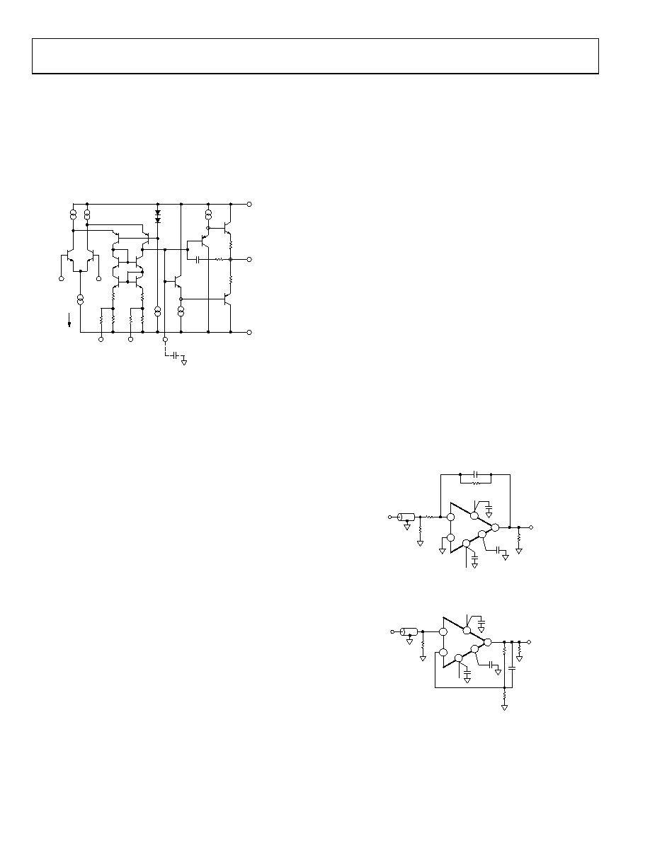
THEORY OF OPERATION
The AD829 is fabricated on the Analog Devices, Inc., proprietary
complementary bipolar (CB) process, which provides PNP and
NPN transistors with similar fTs of 600 MHz. As shown in
Figure 35, the AD829 input stage consists of an NPN differential
pair in which each transistor operates at a 600 A collector current.
This gives the input devices a high transconductance, which in
turn gives the AD829 a low noise figure of 2 nV/√Hz at 1 kHz.
Figure 35. Simplified Schematic
The input stage drives a folded cascode that consists of a fast pair of
PNP transistors. These PNPs drive a current mirror that provides a
differential-input-to-single-ended-output conversion. The high
speed PNPs are also used in the current-amplifying output stage,
which provides a high current gain of 40,000. Even under heavy
loading conditions, the high fTs of the NPN and PNPs, produced
using the CB process, permit cascading two stages of emitter
followers while maintaining 60 phase margin at closed-loop
bandwidths greater than 50 MHz.
Two stages of complementary emitter followers also effectively
buffer the high impedance compensation node (at the CCOMP pin)
from the output so that the AD829 can maintain a high dc open-
loop gain, even into low load impedances (92 dB into a 150
load and 100 dB into a 1 k load). Laser trimming and PTAT
biasing ensure low offset voltage and low offset voltage drift,
enabling the user to eliminate ac coupling in many applications.
For added flexibility, the AD829 provides access to the internal
frequency compensation node. This allows users to customize the
frequency response characteristics for a particular application.
Unity-gain stability requires a compensation capacitance of 68 pF
(Pin 5 to ground), which yields a small signal bandwidth of
66 MHz and slew rate of 16 V/s. The slew rate and gain
bandwidth product varies inversely with compensation
capacitance. Table 4 and Figure 37 show the optimum
compensation capacitance and the resulting slew rate for
a desired noise gain.
For gains between 1 and 20, choose CCOMP to keep the small signal
bandwidth relatively constant. The minimum gain that will still
provide stability depends on the value of the external
compensation capacitance.
An RC network in the output stage (see Figure 35) completely
removes the effect of capacitive loading when the amplifier
compensates for closed-loop gains of 10 or higher. At low
frequencies, and with low capacitive loads, the gain from the
compensation node to the output is very close to unity. In this case,
C is bootstrapped and does not contribute to the compensation
capacitance of the device. As the capacitive load increases, a pole
forms with the output impedance of the output stage, which
reduces the gain, and subsequently, C is incompletely
bootstrapped. Therefore, some fraction of C contributes to the
compensation capacitance, and the unity-gain bandwidth falls.
As the load capacitance is further increased, the bandwidth
continues to fall, and the amplifier remains stable.
EXTERNALLY COMPENSATING THE AD829
The AD829 is stable with no external compensation for noise
gains greater than 20. For lower gains, two different methods of
frequency compensating the amplifier can be used to achieve
closed-loop stability: shunt and current feedback compensation.
SHUNT COMPENSATION
Figure 36 and Figure 37 show that shunt compensation has an
external compensation capacitor, CCOMP, connected between the
compensation pin and ground. This external capacitor is tied in
parallel with approximately 3 pF of internal capacitance at the
compensation node. In addition, a small capacitance, CLEAD, in
parallel with resistor R2, compensates for the capacitance at the
inverting input of the amplifier.
Figure 36. Inverting Amplifier Connection Using External Shunt
Compensation
Figure 37. Noninverting Amplifier Connection Using External Shunt
Compensation
as the corresponding slew rates and bandwidth. The capacitor
values were selected to provide a small signal frequency response
with <1 dB of peaking and <10% overshoot. For Table 4, ±15 V
00880-035
–IN
+IN
1.2mA
OFFSET NULL
C
12.5pF
R
500
OUTPUT
+VS
–VS
CCOMP
15
15
00880-036
2
3
7
6
4
–
+
AD829
+VS
–VS
0.1
F
0.1
F
5
CCOMP
50
50
COAX
CABLE
R1
CLEAD
R2
VOUT
1k
VIN
00880-037
3
2
7
6
4
+
–
AD829
+VS
–VS
0.1
F
0.1
F
CLEAD
5
CCOMP
50
50
CABLE
VOUT
R2
R1
1k
VIN
相关PDF资料 |
PDF描述 |
|---|---|
| VE-B4Z-MX-B1 | CONVERTER MOD DC/DC 2V 30W |
| AD7543JNZ | IC DAC 12BIT SERIAL INPUT 16-DIP |
| VE-B4Z-MW-B1 | CONVERTER MOD DC/DC 2V 40W |
| AD5570ARS-REEL | IC DAC 16BIT SRL IN/VOUT 16-SSOP |
| AD8146ACPZ-R2 | IC DRIVER TRPL DIFF VID 24LFCSP |
相关代理商/技术参数 |
参数描述 |
|---|---|
| AD829ARZ-REEL | 功能描述:IC VIDEO OPAMP HS LN 8-SOIC T/R RoHS:是 类别:集成电路 (IC) >> 线性 - 放大器 - 视频放大器和频缓冲器 系列:- 标准包装:1,000 系列:- 应用:驱动器 输出类型:差分 电路数:3 -3db带宽:350MHz 转换速率:1000 V/µs 电流 - 电源:14.5mA 电流 - 输出 / 通道:60mA 电压 - 电源,单路/双路(±):5 V ~ 12 V,±2.5 V ~ 6 V 安装类型:表面贴装 封装/外壳:20-VFQFN 裸露焊盘 供应商设备封装:20-QFN 裸露焊盘(4x4) 包装:带卷 (TR) |
| AD829ARZ-REEL7 | 功能描述:IC VIDEO OPAMP HS LN 8-SOIC T/R RoHS:是 类别:集成电路 (IC) >> 线性 - 放大器 - 视频放大器和频缓冲器 系列:- 标准包装:1,000 系列:- 应用:驱动器 输出类型:差分 电路数:3 -3db带宽:350MHz 转换速率:1000 V/µs 电流 - 电源:14.5mA 电流 - 输出 / 通道:60mA 电压 - 电源,单路/双路(±):5 V ~ 12 V,±2.5 V ~ 6 V 安装类型:表面贴装 封装/外壳:20-VFQFN 裸露焊盘 供应商设备封装:20-QFN 裸露焊盘(4x4) 包装:带卷 (TR) |
| AD829JCHIPS | 制造商:Analog Devices 功能描述: |
| AD829JN | 功能描述:IC VIDEO OPAMP LN HS 8-DIP RoHS:否 类别:集成电路 (IC) >> 线性 - 放大器 - 视频放大器和频缓冲器 系列:- 标准包装:1,000 系列:- 应用:驱动器 输出类型:差分 电路数:3 -3db带宽:350MHz 转换速率:1000 V/µs 电流 - 电源:14.5mA 电流 - 输出 / 通道:60mA 电压 - 电源,单路/双路(±):5 V ~ 12 V,±2.5 V ~ 6 V 安装类型:表面贴装 封装/外壳:20-VFQFN 裸露焊盘 供应商设备封装:20-QFN 裸露焊盘(4x4) 包装:带卷 (TR) |
| AD829JNAD829JR | 制造商:未知厂家 制造商全称:未知厂家 功能描述:High Speed Low Noise Video Op Amp(336.85 k) |
发布紧急采购,3分钟左右您将得到回复。