- 您现在的位置:买卖IC网 > PDF目录373943 > AD8313-EVAL (Analog Devices, Inc.) 0.1 GHz-2.5 GHz, 70 dB Logarithmic Detector/Controller PDF资料下载
参数资料
| 型号: | AD8313-EVAL |
| 厂商: | Analog Devices, Inc. |
| 英文描述: | 0.1 GHz-2.5 GHz, 70 dB Logarithmic Detector/Controller |
| 中文描述: | 0.1千兆赫,2.5千兆赫,70分贝的对数检测器/控制器 |
| 文件页数: | 8/16页 |
| 文件大小: | 261K |
| 代理商: | AD8313-EVAL |
AD8313
–8–
REV. B
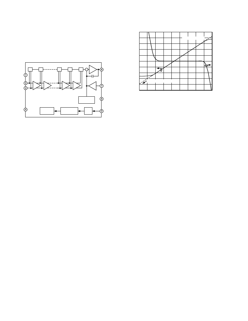
CIRCUIT DESCRIPTION
The AD8313 is essentially an 8-stage logarithmic amplifier,
specifically designed for use in RF measurement and power
amplifier control applications at frequencies up to 2.5 GHz. A
block diagram is shown in Figure 20. (For a full treatment of
log-amp theory and design principles, consult the AD8307
data sheet).
+
+
+
+
AD8313
VOUT
VSET
COMM
PWDN
GAIN
BIAS
BAND-GAP
REFERENCE
SLOPE
CONTROL
INTERCEPT
CONTROL
EIGHT 8dB 3.5GHz AMPLIFIER STAGES
8dB
8dB
VPOS
INHI
INLO
VPOS
8dB
8dB
NINE DETE+
C
INT
LP
I
v
V
V
v
I
Figure 20. Block Diagram
A fully-differential design is used, and the inputs INHI and INLO
(Pins 2 and 3) are internally biased to approximately 0.75 V
below the supply voltage, and present a low frequency imped-
ance of nominally 900
in parallel with 1.1 pF. The noise
spectral density referred to the input is 0.6 nV/
√
Hz
, equivalent
to a voltage of 35
μ
V rms in a 3.5 GHz bandwidth, or a noise
power of –76 dBm re: 50
. This sets the lower limit to the
dynamic range; the Applications section shows how to increase
the sensitivity by the use of a matching network or input trans-
former. However, the low end accuracy of the AD8313 is enhanced
by specially shaping the demodulation transfer characteristic to
partially compensate for errors due to internal noise.
Each of the eight cascaded stages has a nominal voltage gain of
8 dB and a bandwidth of 3.5 GHz, and is supported by preci-
sion biasing cells which determine this gain and stabilize it
against supply and temperature variations. Since these stages are
direct-coupled and the dc gain is high, an offset-compensation
loop is included. The first four of these stages, and the biasing
system, are powered from Pin 4, while the later stages and the
output interfaces are powered from Pin 1. The biasing is con-
trolled by a logic interface PWDN (Pin 5); this is grounded for
normal operation, but may be taken high (to V
S
) to disable the
chip. The threshold is at V
POS
/2 and the biasing functions are
enabled and disabled within 1.8
μ
s.
Each amplifier stage has a detector cell associated with its out-
put. These nonlinear cells essentially perform an absolute-value
(full-wave rectification) function on the differential voltages
along this backbone, in a transconductance fashion; their out-
puts are in current-mode form and are thus easily summed. A
ninth detector cell is added at the input of the AD8313. Since
the mid-range response of each of these nine detector stages is
separated by 8 dB, the overall dynamic range is about 72 dB
(Figure 21). The upper end of this range is determined by the
capacity of the first detector cell, and occurs at approximately
0 dBm. The practical dynamic range is over 70 dB, to the
±
3 dB error points. However, some erosion of this range will
occur at temperature and frequency extremes. Useful operation to
over 3 GHz is possible, and the AD8313 remains serviceable at
10 MHz (see Typical Performance Characteristics), needing
only a small amount of additional ripple filtering.
INPUT AMPLITUDE – dBm
2.0
–80
V
O
1.8
1.6
1.4
1.2
1.0
0.8
0.6
0.4
0.2
0
–70
–60
–50
–40
–30
–20
–10
0
5
4
3
2
1
0
–1
–2
–3
–4
–5
E
–90
INTERCEPT = –100dBm
SLOPE = 18mV/dB
Figure 21. Typical RSSI Response and Error vs. Input
Power at 1.9 GHz
The fluctuating current output generated by the detector cells,
with a fundamental component at twice the signal frequency, is
filtered first by a low-pass section inside each cell, and also by
the output stage. The output stage converts these currents to a
voltage, V
OUT
, at pin VOUT (Pin 8), which can swing “rail-to-
rail.” The filter exhibits a two-pole response with a corner at
approximately 12 MHz and full-scale rise time (10%–90%) of
40 ns. The residual output ripple at an input frequency of
100 MHz has an amplitude of under 1 mV. The output can
drive a small resistive load: it can source currents of up to
400
μ
A, and sink up to 10 mA. The output is stable with any
capacitive load, though settling time may be impaired. The low
frequency incremental output impedance is approximately 0.2
.
In addition to its use as an RF power measurement device (that
is, as a logarithmic amplifier) the AD8313 may also be used in
controller applications, by breaking the feedback path from
VOUT to the VSET
(Pin 7), which determines the slope of the
output (nominally 18 mV/dB). This pin becomes the setpoint
input in controller modes. In this mode, the voltage V
OUT
re-
mains close to ground (typically under 50 mV) until the decibel
equivalent of the voltage V
SET
is reached at the input, when
V
OUT
makes a rapid transition to a voltage close to V
POS
(see
controller mode). The logarithmic intercept is nominally posi-
tioned at –100 dBm (re: 50
) and this is effective in both the
log amp mode and the controller mode.
Thus, with Pins 7 and 8 connected (log amp mode) we have:
V
OUT
=
V
SLOPE
(P
IN
+
100
dBm)
where
P
IN
is the input power, stated in dBm when the source is
directly terminated in 50
. However, the input impedance of
the AD8313 is much higher than 50
and the sensitivity of this
device may be increased by about 12 dB by using some type of
matching network (see below), which adds a voltage gain and
lowers the intercept by the same amount. This dependence on
the choice of reference impedance can be avoided by restating
the expression as:
V
OUT
=
20
×
V
SLOPE
×
log
(V
IN
/
2.2
μ
V)
where
V
IN
is the rms value of a sinusoidal input appearing
across Pins 2 and 3; here, 2.2
μ
V corresponds to the intercept,
expressed in voltage terms. (For a more thorough treatment of
the effect of signal waveform and metrics on the intercept posi-
tioning for a log amp, see the AD8307 data sheet).
相关PDF资料 |
PDF描述 |
|---|---|
| AD8313 | 0.1 GHz-2.5 GHz,70dB Logarithmic Detector/Controller(频率为0.1 GHz-2.5 GHz,增益为70dB的对数检测器/控制器) |
| AD8314ARM | 100 MHz-2500 MHz 45 dB RF Detector/Controller |
| AD8314ARM-REEL | 100 MHz-2500 MHz 45 dB RF Detector/Controller |
| AD8314ARM-REEL7 | 100 MHz-2500 MHz 45 dB RF Detector/Controller |
| AD8314 | 100 MHz-2500 MHz 45 dB RF Detector/Controller |
相关代理商/技术参数 |
参数描述 |
|---|---|
| AD8313-EVALZ | 制造商:Analog Devices 功能描述:EVAL BOARD - Bulk |
| AD8314 | 制造商:AD 制造商全称:Analog Devices 功能描述:100 MHz to 2.7 GHz, 45 dB RF Detector/Controller |
| AD8314_06 | 制造商:AD 制造商全称:Analog Devices 功能描述:100 MHz to 2.7 GHz, 45 dB RF Detector/Controller |
| AD8314ACP-EVAL | 制造商:Analog Devices 功能描述:EVAL BD 100 MHZ TO 2.7 GHZ, 45 DB RF DETECTOR/CNTRLR - Bulk |
| AD8314ACP-EVALZ | 制造商:Analog Devices 功能描述:AD8314 RF DETECTOR EVAL BOARD 制造商:Analog Devices 功能描述:AD8314, RF DETECTOR, EVAL BOARD 制造商:Analog Devices 功能描述:AD8314, RF DETECTOR, EVAL BOARD, Silicon Manufacturer:Analog Devices, Silicon Co 制造商:Analog Devices 功能描述:AD8314, RF DETECTOR, EVAL BOARD, Silicon Manufacturer:Analog Devices, Silicon Core Number:(Not Applicable), Kit Application Type:(Not Available), Application Sub Type:-, SVHC:No SVHC (20-Jun-2013) , RoHS Compliant: Yes |
发布紧急采购,3分钟左右您将得到回复。