- 您现在的位置:买卖IC网 > PDF目录373943 > AD8318-EVAL (Analog Devices, Inc.) 1 MHz - 8 GHz, 60 dB Logarithmic Detector/Controller PDF资料下载
参数资料
| 型号: | AD8318-EVAL |
| 厂商: | Analog Devices, Inc. |
| 英文描述: | 1 MHz - 8 GHz, 60 dB Logarithmic Detector/Controller |
| 中文描述: | 1兆赫- 8千兆赫,60分贝对数检测器/控制器 |
| 文件页数: | 18/24页 |
| 文件大小: | 2127K |
| 代理商: | AD8318-EVAL |
AD8318
can be increased by placing a resistor divider between VOUT
and VSET (i.e., one resistor from VOUT to VSET and one
resistor from VSET to common). For example, if two equal
resistors are used (e.g., 10 k/10 k), the slope will double to
approximately
50 mV/dB. The input impedance of VSET is
approximately 500 k. Slope setting resistors should be kept
below ~50 k to prevent this input impedance from affecting
the resulting slope. When increasing the slope, the new output
voltage range cannot exceed the output voltage swing capability
of the output stage. Refer to the Measurement Mode section of
the data sheet.
Rev. 0 | Page 18 of 24
0
VOUT
AD8318
50mV/dB
VSET
10k
10k
Figure 36. Increasing the Slope
RESPONSE TIME CAPABILITY
The AD8318 has a 10 ns rise/fall time capability (10% – 90%) for
input power switching between the noise floor and
0 dBm. This capability enables RF burst measurements at
repetition rates to beyond 60 MHz. In most measurement
applications, the AD8318 will have an external capacitor
connected to CLPF to provide additional filtering for VOUT.
However, the use of the CLPF capacitor slows the response time
as does stray capacitance on VOUT. For an application requiring
maximum RF burst detection capability, the CLPF capacitor pin
should be left unconnected. In this case, the integration function
is provided by the 700 fF on-chip capacitor.
There is a 10 internal resistor in series with the output driver,
an external 40 back-terminating resistor should be added in
series at the output when driving a 50 coaxial cable. The back-
terminating resistor should be placed close to the VOUT pin.
The AD8318 has the drive capability to drive a 50 load at the
end of the coaxial cable or transmission line when back
terminated. See Figure 37.
The circuit diagram in Figure 37 shows the AD8318 used with a
high speed comparator circuit. The 40 series resistor at the
output of the AD8318 combines with an internal 10 to
properly match to the 50 input of the comparator.
0
PUINPUT
1nF
+5V
40
100
100
50
50
1nF
52.3
INHI
INLO
VOUT
VPOS
GND
AD8318
VSET
ADCMP563
+5V
–5.2V
–5.2V
V
REF
= 1.8V–1.2V
50
50
COOUTPUT
AD8318
Figure 37. AD8318 Operating with the High Speed ADCMP563 Comparator
0
0
100
200
300
400
500
600
700
800
TIME (ns)
AD8318
COMPARATOR
PUINPUT
–50dB
–30dB
–20dB
–10dB
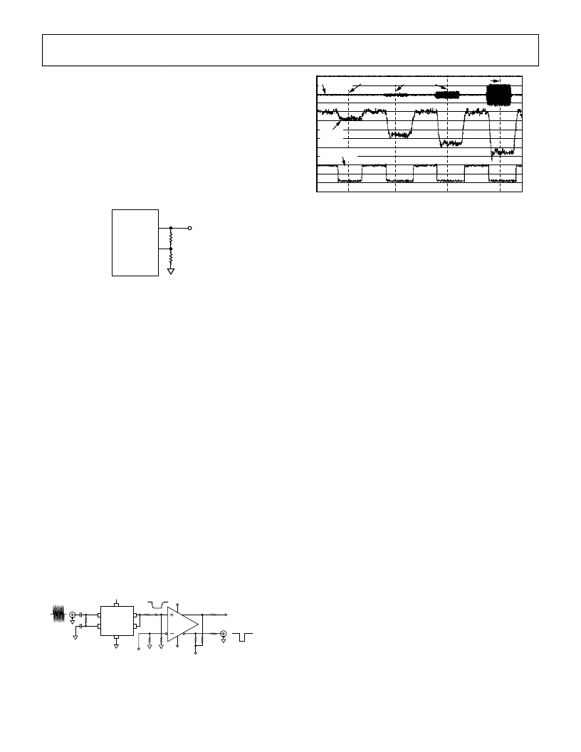
Figure 38. Pulse Response of AD8318 and Comparator for RF Pulses of
Varying Amplitudes
Figure 38 shows the response of the AD8318 and the
comparator for a 500 MHz pulsed sine wave of varying
amplitudes. The output level of the AD8318 is the signal
strength of the input signal. For applications where these RF
bursts are very small, the output level will not change by a
large amount. Using a comparator is beneficial because it
will turn the output of the log amp into a limiter-like signal.
CONTROLLER MODE
The AD8318 provides a controller mode feature at the
VOUT pin. Using V
SET
for the setpoint voltage, it is possible
for the AD8318 to control subsystems, such as power
amplifiers (PAs), variable gain amplifiers (VGAs), or
variable voltage attenuators (VVAs) that have output power
that increases monotonically with respect to their gain
control signal.
To operate in controller mode, the link between VSET and
VOUT is broken. A setpoint voltage is applied to the VSET
input; VOUT is connected to the gain control terminal of
the VGA and the detector’s RF input is connected to the
output of the VGA (usually using a directional coupler and
some additional attenuation). Based on the defined
relationship between V
OUT
and the RF input signal when the
device is in measurement mode, the AD8318 will adjust the
voltage on VOUT (VOUT is now an error amplifier output)
until the level at the RF input corresponds to the applied
V
SET
. When the AD8318 operates in controller mode, there
is no defined relationship between V
SET
and V
OUT
voltage;
V
OUT
will settle to a value that results in the correct input
signal level appearing at INHI/INLO.
In order for this output power control loop to be stable,
a ground-referenced capacitor must be connected to the
C
FLT
pin.
This capacitor integrates the error signal (which is actually a
current) that is present when the loop is not balanced.
相关PDF资料 |
PDF描述 |
|---|---|
| AD8318 | 1 MHz - 8 GHz, 60 dB Logarithmic Detector/Controller |
| AD8318ACPZ-REEL7 | 1 MHz - 8 GHz, 60 dB Logarithmic Detector/Controller |
| AD8321AR-REEL | Gain Programmable CATV Line Driver |
| AD8321-EVAL | Gain Programmable CATV Line Driver |
| AD8321AR | Gain Programmable CATV Line Driver |
相关代理商/技术参数 |
参数描述 |
|---|---|
| AD8318-EVALZ | 功能描述:BOARD EVAL FOR AD8318 RoHS:是 类别:RF/IF 和 RFID >> RF 评估和开发套件,板 系列:- 标准包装:1 系列:- 类型:GPS 接收器 频率:1575MHz 适用于相关产品:- 已供物品:模块 其它名称:SER3796 |
| AD8318SCPZ-EP-R2 | 制造商:Analog Devices 功能描述:1 MHZ TO 8 GHZ, 70 DB LOGARITHMIC DETECTOR / CONTROLLER - Tape and Reel |
| AD8318SCPZ-EP-RL7 | 制造商:Analog Devices 功能描述: |
| AD8318SCPZ-EP-WP | 制造商:Analog Devices 功能描述:1 MHZ TO 8 GHZ, 70 DB LOGARITHMIC DETECTOR / CONTROLLER - Waffle Pack |
| AD8318XCPZ | 制造商:Analog Devices 功能描述:100MHZ - 8GHZ, 70DB LOGARITHMIC DETECTOR/CONTROLLER - Bulk |
发布紧急采购,3分钟左右您将得到回复。