- 您现在的位置:买卖IC网 > PDF目录373943 > AD8321AR-REEL (ANALOG DEVICES INC) Gain Programmable CATV Line Driver PDF资料下载
参数资料
| 型号: | AD8321AR-REEL |
| 厂商: | ANALOG DEVICES INC |
| 元件分类: | 通用总线功能 |
| 英文描述: | Gain Programmable CATV Line Driver |
| 中文描述: | LINE DRIVER, PDSO20 |
| 封装: | MS-013AC, SOIC-20 |
| 文件页数: | 9/19页 |
| 文件大小: | 660K |
| 代理商: | AD8321AR-REEL |
AD8321
–9–
REV. 0
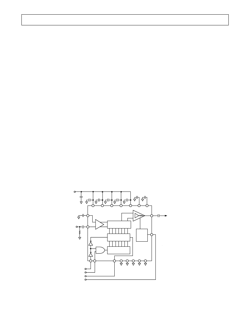
Basic Connection
Figure 25 shows the basic schematic for operating the AD8321
in single-ended inverting mode. To operate in inverting mode,
connect the input signal through an ac coupling capacitor to
VIN–; VIN+ should be decoupled to ground with a 0.1
μ
F
capacitor. Because the amplifier operates from a single supply,
and the differential input pins are biased to approximately
V
CC
/2, the differential inputs must be ac-coupled using 0.1
μ
F
capacitors. For operation in the noninverting mode, the VIN–
pin should be decoupled to ground via a 0.1
μ
F capacitor, with
the input signal being fed to the AD8321 through the (ac-coupled)
VIN+ pin. Inverting mode should be chosen if the AD8321 is
being used as a drop-in replacement for the AD8320 (the
AD8321 predecessor). Balanced differential inputs to the
AD8321 may also be applied at an amplitude that is one-half
the specified single-ended input amplitude. See the Differential
Inputs section for more on this mode of operation.
Power Supply and Decoupling
The AD8321 should be powered with a good quality (i.e., low
noise) single supply of 9 V. Although the AD8321 circuit will
function at voltages lower than 9 V, optimum performance will
not be achieved at lower supply settings. Careful attention must
be paid to decoupling the power supply pins. A 10
μ
F capacitor
located in near proximity to the AD8321 is required to provide
good decoupling for lower frequency signals. In addition, and
more importantly, five 0.1
μ
F decoupling capacitors should be
located close to each of the five power supply pins (7, 8, 9, 17
and 20). A 0.1
μ
F capacitor must also be connected to the pins
labeled BYP1 and BYP2 (Pins 5 and 14) to provide decoupling
to internal nodes of the device. All six ground pins should be
connected to a common low impedance ground plane.
Input Bias, Impedance and Termination
On the input side, the VIN+ and VIN– have a dc bias level
equal to (V
CC
/2)–0.2 V. The input signal must therefore be ac-
coupled before being applied to either input pin. The input
impedance, when operated in single-ended mode is roughly
820
(900
in differential mode). An external shunt resis-
tance (R1) to ground of 82.5
is required to create a single-
ended input impedance of close to 75
. If single-ended 50
termination is required, a 53.6
shunt resistor may be used.
Differential input operation may be achieved by using a shunt
resistor of 41
to ground on each of the inputs, or 82.6
across the inputs resulting in a differential input impedance of
approximately 75
. Note: to avoid dc loading of either the
VIN+ or VIN– pin, the ac-coupling capacitor must be placed
between the input pin(s) and the shunt resistor(s). Refer to the
Differential Inputs section for more details on this mode of
operation.
Output Bias, Impedance and Termination
On the output side, the VOUT pin is also dc-biased to V
CC
/2 or
midway between the supply voltage and ground. The output
signal must therefore be ac-coupled before being applied to the
load. The dc-bias voltage is available on the BYP1 and BYP2
pins (Pins 5 and 14 respectively) and can be used in dc-biasing
schemes. These nodes must be decoupled to ground using a
0.1
μ
F capacitor as shown in Figure 25. If the BYP1 and/or
BYP2 voltages are used externally, they should be buffered.
External back termination resistors are not required when using
the AD8321. The output impedance of the AD8321 is 75
and
is maintained dynamically. This on chip back termination is
maintained regardless of whether the amplifier is in forward
transmit mode or reverse powered down mode. If the output
signal is being evaluated on 50
test equipment such as a spec-
trum analyzer, a 75
to 50
adapter (commonly called a mini-
mum loss pad) should be used to maintain a properly matched
circuit.
ATTENUATOR
CORE
DATA SHIFT
REGISTER
DATA LATCH
AD8321
POWER-
DOWN/
SWITCH
INTER
DATEN
CLK
VIN+
VIN–
PD
VOUT
SDATA
VCC
VCC
C8
0.1
m
F
VCC
C9
0.1
m
F
VCC
C10
0.1
m
F
VCC
C11
0.1
m
F
BYP1
C5
0.1
m
F
C2
0.1
m
F
C1
0.1
m
F
R1
82.5
V
INPUT
DATEN
CLK
SDATA
GND
GND
GND
GND
GND
C4
0.1
m
F
TO
DIPLEXER
R
IN
= 75
V
BYP2
VCC
+9V
Ce
0.1
m
F
C6
10
m
F
C7
0.1
m
F
Figure 25. Basic Connection for Single-Ended Inverting Operation
相关PDF资料 |
PDF描述 |
|---|---|
| AD8321-EVAL | Gain Programmable CATV Line Driver |
| AD8321AR | Gain Programmable CATV Line Driver |
| AD8322ARU-REEL | 5 V CATV Line Driver Coarse Step Output Power Control |
| AD8322-EVAL | 5 V CATV Line Driver Coarse Step Output Power Control |
| AD8322ARU | 5 V CATV Line Driver Coarse Step Output Power Control |
相关代理商/技术参数 |
参数描述 |
|---|---|
| AD8321ARZ | 功能描述:IC LINE DRIVER CATV 3.3V 20SOIC RoHS:是 类别:集成电路 (IC) >> 线性 - 视频处理 系列:- 产品变化通告:Product Discontinuation 07/Mar/2011 标准包装:3,000 系列:OMNITUNE™ 类型:调谐器 应用:移动电话,手机,视频显示器 安装类型:表面贴装 封装/外壳:65-WFBGA 供应商设备封装:PG-WFSGA-65 包装:带卷 (TR) 其它名称:SP000365064 |
| AD8321ARZ2 | 制造商:AD 制造商全称:Analog Devices 功能描述:Gain Programmable CATV Line DRiver |
| AD8321ARZ-REEL | 功能描述:IC LINE DVR CATV 20-SOIC T/R RoHS:是 类别:集成电路 (IC) >> 线性 - 视频处理 系列:- 产品变化通告:Product Discontinuation 07/Mar/2011 标准包装:3,000 系列:OMNITUNE™ 类型:调谐器 应用:移动电话,手机,视频显示器 安装类型:表面贴装 封装/外壳:65-WFBGA 供应商设备封装:PG-WFSGA-65 包装:带卷 (TR) 其它名称:SP000365064 |
| AD8321ARZ-REEL2 | 制造商:AD 制造商全称:Analog Devices 功能描述:Gain Programmable CATV Line DRiver |
| AD8321-EVAL | 功能描述:BOARD EVAL FOR AD8321 RoHS:否 类别:编程器,开发系统 >> 评估演示板和套件 系列:- 产品培训模块:Obsolescence Mitigation Program 标准包装:1 系列:- 主要目的:电源管理,电池充电器 嵌入式:否 已用 IC / 零件:MAX8903A 主要属性:1 芯锂离子电池 次要属性:状态 LED 已供物品:板 |
发布紧急采购,3分钟左右您将得到回复。