- 您现在的位置:买卖IC网 > PDF目录373943 > AD8322ARU-REEL (ANALOG DEVICES INC) 5 V CATV Line Driver Coarse Step Output Power Control PDF资料下载
参数资料
| 型号: | AD8322ARU-REEL |
| 厂商: | ANALOG DEVICES INC |
| 元件分类: | 通用总线功能 |
| 英文描述: | 5 V CATV Line Driver Coarse Step Output Power Control |
| 中文描述: | LINE DRIVER, PDSO28 |
| 封装: | TSSOP-28 |
| 文件页数: | 4/16页 |
| 文件大小: | 243K |
| 代理商: | AD8322ARU-REEL |
REV. 0
AD8322
–4–
ORDERING GUIDE
Model
Temperature Range
–40
°
C to +85
°
C
–40
°
C to +85
°
C
Package Description
JA
Package Option
AD8322ARU
AD8322ARU-REEL
AD8322-EVAL
28-Lead TSSOP
28-Lead TSSOP
Evaluation Board
67.7
°
C/W
*
67.7
°
C/W
*
RU-28
RU-28
*
Thermal Resistance measured on SEMI standard 4-layer board.
ABSOLUTE MAXIMUM RATINGS
*
Supply Voltage +V
S
Pins 6, 8, 9, 20, 21, 23, 27 . . . . . . . . . . . . . . . . . . . . . . . 6 V
Input Voltages
Pins 25, 26 . . . . . . . . . . . . . . . . . . . . . . . . . . . . . . . .
±
0.5 V
Pins 1, 2, 3, 7 . . . . . . . . . . . . . . . . . . . . . . . –0.8 V to +5.5 V
Internal Power Dissipation
TSSOP (RU) . . . . . . . . . . . . . . . . . . . . . . . . . . . . . . 0.90 W
Operating Temperature Range . . . . . . . . . . . –40
°
C to +85
°
C
Storage Temperature Range . . . . . . . . . . . . –65
°
C to +150
°
C
Lead Temperature, Soldering 60 seconds . . . . . . . . . . . 300
°
C
*
Stresses above those listed under Absolute Maximum Ratings may cause perma-
nent damage to the device. This is a stress rating only; functional operation of the
device at these or any other conditions above those indicated in the operational
section of this specification is not implied. Exposure to absolute maximum rating
conditions for extended periods may affect device reliability.
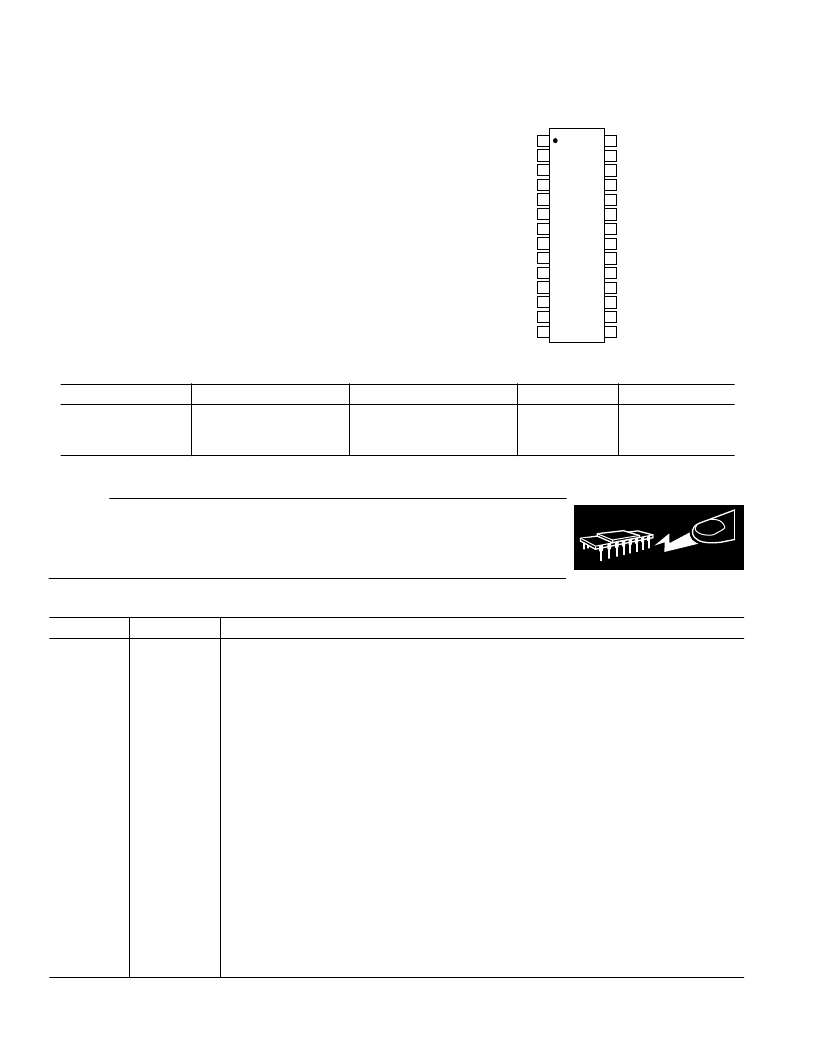
PIN CONFIGURATION
TOP VIEW
(Not to Scale)
28
27
26
25
24
23
22
21
20
19
18
17
16
15
1
2
3
4
5
6
7
8
9
10
11
12
13
14
AD8322
DATEN
GND
SDATA
VCC
CLK
VIN
–
GND
VIN+
VCC
GND
PD
VCC
GND
GND
GND
VCC
VCC
VCC
VCC
GND
GND
GND
GND
GND
GND
OUT
–
OUT+
BYP
CAUTION
ESD (electrostatic discharge) sensitive device. Electrostatic charges as high as 4000 V readily
accumulate on the human body and test equipment and can discharge without detection. Although
the AD8322 features proprietary ESD protection circuitry, permanent damage may occur on
devices subjected to high-energy electrostatic discharges. Therefore, proper ESD precautions are
recommended to avoid performance degradation or loss of functionality.
WARNING!
ESD SENSITIVE DEVICE
PIN FUNCTION DESCRIPTIONS
Pin No.
Mnemonic
Description
1
SDATA
Serial Data Input. This digital input allows for an 8-bit serial (gain) word to be loaded into the internal
register with the MSB (Most Significant Bit) first.
Clock Input. The clock port controls the serial attenuator data transfer rate to the 8-bit master-slave
register. A Logic 0-to-1 transition latches the data bit and a 1-to-0 transfers the data bit to the slave.
This requires the input serial data word to be valid at or before this clock transition.
Data Enable Low Input. This port controls the 8-bit parallel data latch and shift register. A Logic 0-to-1
transition transfers the latched data to the attenuator core (updates the gain) and simultaneously inhibits
serial data transfer into the register. A 1-to-0 transition inhibits the data latch (holds the previous gain
state) and simultaneously enables the register for serial data load.
Common External Ground Reference.
2
CLK
3
DATEN
4, 11, 12, 13,
14, 15, 16, 17,
18, 22, 24, 28
5
6, 8, 9, 20,
21, 23, 27
7
10
19
25
GND
BYP
VCC
Internal Bypass. This pin must be externally ac-decoupled (0.1
μ
F capacitor).
Common Positive External Supply Voltage. A 0.1
μ
F capacitor must decouple each pin.
PD
OUT–
OUT+
VIN+
Logic “0” powers down the part. Logic “1” powers up the part.
Negative Output Signal.
Positive Output Signal.
Noninverting Input. DC-biased to approximately V
CC
/2. Refer to Applications section for proper
termination.
Inverting Input. DC-biased to approximately V
CC
/2. Refer to Applications section for proper termination.
26
VIN–
相关PDF资料 |
PDF描述 |
|---|---|
| AD8322-EVAL | 5 V CATV Line Driver Coarse Step Output Power Control |
| AD8322ARU | 5 V CATV Line Driver Coarse Step Output Power Control |
| AD8322 | 5 V CATV Line Driver Coarse Step Output Power Control |
| AD8323ARU-REEL | 5 V CATV Line Driver Fine Step Output Power Control |
| AD8323ARU | 5 V CATV Line Driver Fine Step Output Power Control |
相关代理商/技术参数 |
参数描述 |
|---|---|
| AD8322ARUZ | 制造商:Analog Devices 功能描述:SP Amp Line Driver Amp Single 5.25V 28-Pin TSSOP Tube |
| AD8322ARUZ-REEL | 功能描述:IC LN DVR CATV COARS-STP 28TSSOP RoHS:是 类别:集成电路 (IC) >> 线性 - 视频处理 系列:- 产品变化通告:Product Discontinuation 07/Mar/2011 标准包装:3,000 系列:OMNITUNE™ 类型:调谐器 应用:移动电话,手机,视频显示器 安装类型:表面贴装 封装/外壳:65-WFBGA 供应商设备封装:PG-WFSGA-65 包装:带卷 (TR) 其它名称:SP000365064 |
| AD8322-EVAL | 制造商:Analog Devices 功能描述:Evaluation Kit For 5 V CATV Line Driver Coarse Step Output Power Control |
| AD8323 | 制造商:AD 制造商全称:Analog Devices 功能描述:5 V CATV Line Driver Fine Step Output Power Control |
| AD8323ARU | 制造商:Analog Devices 功能描述:SP Amp Line Driver Amp Single 5.25V 28-Pin TSSOP Tube 制造商:Rochester Electronics LLC 功能描述:TSSOP FINE STEP +5V CATV LINE DRIVER - Bulk |
发布紧急采购,3分钟左右您将得到回复。