- 您现在的位置:买卖IC网 > PDF目录373943 > AD8322ARU-REEL (ANALOG DEVICES INC) 5 V CATV Line Driver Coarse Step Output Power Control PDF资料下载
参数资料
| 型号: | AD8322ARU-REEL |
| 厂商: | ANALOG DEVICES INC |
| 元件分类: | 通用总线功能 |
| 英文描述: | 5 V CATV Line Driver Coarse Step Output Power Control |
| 中文描述: | LINE DRIVER, PDSO28 |
| 封装: | TSSOP-28 |
| 文件页数: | 8/16页 |
| 文件大小: | 243K |
| 代理商: | AD8322ARU-REEL |
REV. 0
AD8322
–8–
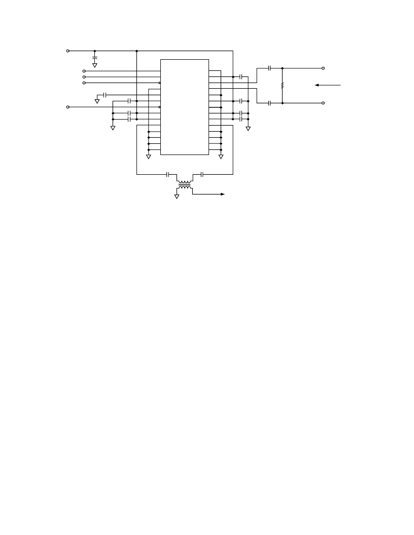
Output Bias, Impedance, and Termination
The differential output pins V
OUT+
and V
OUT
–
are also biased to
a dc level of approximately V
CC
/2. Therefore, the outputs should
be ac-coupled before being applied to the load. This may be
accomplished by connecting 0.1
μ
F capacitors in series with the
outputs as shown in the typical applications circuit of Figure 6.
The differential output impedance of the AD8322 is internally
maintained at 75
, regardless of whether the amplifier is in
forward transmit mode or reverse power-down mode, elimi-
nating the need for external back termination resistors. A 1:1
transformer (TOKO #617DB-A0070) is used to couple the
amplifier
’
s differential output to the coaxial cable while main-
taining a proper impedance match. If the output signal is being
evaluated on standard 50
test equipment, a 75
to 50
pad must be used to provide the test circuit with the correct
impedance match.
Power Supply Decoupling, Grounding, and Layout
Considerations
Careful attention to printed circuit board layout details will
prevent problems due to associated board parasitics. Proper RF
design technique is mandatory. The 5 V supply power should be
delivered to each of the VCC pins via a low impedance power bus
to ensure that each pin is at the same potential. The power bus
should be decoupled to ground with a 10
μ
F tantalum capacitor
located in close proximity to the AD8322. In addition to the
10
μ
F capacitor, each VCC pin should be individually decoupled
to ground with a 0.1
μ
F ceramic chip capacitor located as close
to the pin as possible. The pin labeled BYP (Pin 5) should also
be decoupled with a 0.1
μ
F capacitor. The PCB should have a
low impedance ground plane covering all unused portions of the
component side of the board, except in the area of the input and
output traces (see Figure 11). It is important to connect all of
the AD8322 ground pins to ensure proper grounding of all
internal nodes. The differential input and output traces should
be kept as short and as symmetrical as possible. In addition, the
input and output traces should be kept far apart in order to
minimize coupling (crosstalk) through the board. Following these
guidelines will improve the overall performance of the AD8322
in all applications.
Initial Power-Up
When the 5 V supply is first applied to the VCC pins of the
AD8322, the gain setting of the amplifier is indeterminate.
Therefore, as power is first applied to the amplifier, the
PD
pin
should be held low (Logic 0) thus preventing forward signal
transmission. After power has been applied to the amplifier, the
gain can be set to the desired level by following the procedure in
the SPI Programming and Gain Adjustment section. The
PD
pin
can then be brought from Logic 0 to 1, enabling forward signal
transmission at the desired gain level.
Asynchronous Power-Down
The asynchronous
PD
pin is used to place the AD8322 into
“
Between Burst
”
mode while maintaining a differential output
impedance of 75
. Applying a Logic 0 to the
PD
pin activates
the on-chip reverse amplifier, providing a 52% reduction in con-
sumed power. The supply current is reduced from approximately
113 mA to approximately 54 mA. In this mode of operation,
between burst noise is minimized and the amplifier can no longer
transmit in the upstream direction.
Distortion, Adjacent Channel Power, and DOCSIS
In order to deliver 58 dBmV of high-fidelity output power
required by DOCSIS, the PA should be able to deliver about
60 to 61 dBmV in order to make up for losses associated with the
transformer and diplexer. It should be noted that the AD8322
was characterized with the TOKO 617DB-A0070 transformer.
TPC 7 and TPC 8 show the AD8322 second and third harmonic
distortion performance versus fundamental frequency for vari-
ous output power levels. These figures are useful for determining
the in-band harmonic levels from 5 MHz to 65 MHz. Harmonics
higher in frequency will be sharply attenuated by the low-pass
filter function of the diplexer. Another measure of signal integ-
rity is adjacent channel power or ACP. DOCSIS section 4.2.9.1.1
states,
“
Spurious emissions from a transmitted carrier may occur
SDATA
CLK
DATEN
GND1
BYP
VCC
PD
VCC1
VCC2
OUT
–
GND2
GND3
GND4
GND5
GND12
VCC6
VIN
–
VIN+
GND11
VCC5
GND10
VCC4
VCC3
OUT+
GND9
GND8
GND7
GND6
AD8322TSSOP
5V
PD
DATEN
SDATA
CLK
10 F
25V
0.1 F
0.1 F
0.1 F
0.1 F
0.1 F
TOKO 617DB-A0070
TO DIPLEXER
Z
IN
= 75
0.1 F
0.1 F
0.1 F
0.1 F
0.1 F
432
V
IN
–
V
IN+
Z
IN
= 150
28
27
26
25
24
23
22
21
20
19
18
17
16
15
1
2
3
4
5
6
7
8
9
10
11
12
13
14
0.1 F
0.1 F
Figure 6. Typical Applications Circuit
相关PDF资料 |
PDF描述 |
|---|---|
| AD8322-EVAL | 5 V CATV Line Driver Coarse Step Output Power Control |
| AD8322ARU | 5 V CATV Line Driver Coarse Step Output Power Control |
| AD8322 | 5 V CATV Line Driver Coarse Step Output Power Control |
| AD8323ARU-REEL | 5 V CATV Line Driver Fine Step Output Power Control |
| AD8323ARU | 5 V CATV Line Driver Fine Step Output Power Control |
相关代理商/技术参数 |
参数描述 |
|---|---|
| AD8322ARUZ | 制造商:Analog Devices 功能描述:SP Amp Line Driver Amp Single 5.25V 28-Pin TSSOP Tube |
| AD8322ARUZ-REEL | 功能描述:IC LN DVR CATV COARS-STP 28TSSOP RoHS:是 类别:集成电路 (IC) >> 线性 - 视频处理 系列:- 产品变化通告:Product Discontinuation 07/Mar/2011 标准包装:3,000 系列:OMNITUNE™ 类型:调谐器 应用:移动电话,手机,视频显示器 安装类型:表面贴装 封装/外壳:65-WFBGA 供应商设备封装:PG-WFSGA-65 包装:带卷 (TR) 其它名称:SP000365064 |
| AD8322-EVAL | 制造商:Analog Devices 功能描述:Evaluation Kit For 5 V CATV Line Driver Coarse Step Output Power Control |
| AD8323 | 制造商:AD 制造商全称:Analog Devices 功能描述:5 V CATV Line Driver Fine Step Output Power Control |
| AD8323ARU | 制造商:Analog Devices 功能描述:SP Amp Line Driver Amp Single 5.25V 28-Pin TSSOP Tube 制造商:Rochester Electronics LLC 功能描述:TSSOP FINE STEP +5V CATV LINE DRIVER - Bulk |
发布紧急采购,3分钟左右您将得到回复。