- 您现在的位置:买卖IC网 > PDF目录10618 > AD8324JRQZ-REEL7 (Analog Devices Inc)IC LINE DRIVER CBL 3.3V 20QSOP PDF资料下载
参数资料
| 型号: | AD8324JRQZ-REEL7 |
| 厂商: | Analog Devices Inc |
| 文件页数: | 5/16页 |
| 文件大小: | 0K |
| 描述: | IC LINE DRIVER CBL 3.3V 20QSOP |
| 标准包装: | 1 |
| 类型: | 线路驱动器,发射器 |
| 应用: | 调制解调器,CATV |
| 安装类型: | 表面贴装 |
| 封装/外壳: | 20-SSOP(0.154",3.90mm 宽) |
| 供应商设备封装: | 20-QSOP |
| 包装: | 标准包装 |
| 其它名称: | AD8324JRQZ-REEL7DKR |
Data Sheet
AD8324
Rev. B | Page 13 of 16
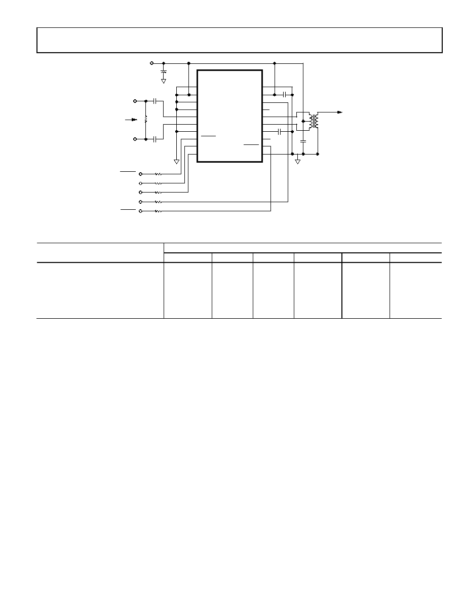
Figure 23. Typical Application Circuit
Table 7. Adjacent Channel Power
Adjacent Channel Symbol Rate (kSym/s)
Channel Symbol Rate (kSym/s)
160
320
640
1280
2560
5120
160
–63
–64
–68
–71
–72
–66
320
–63
–64
–66
–70
–72
–67
640
–64
–65
–67
–71
–67
1280
–67
–65
–66
–68
–67
2560
–70
–67
–66
–67
–65
5120
–72
–70
–67
–64
POWER SUPPLY
Deliver the 3.3 V supply to each of the VCC pins via a low imped-
ance power bus. This ensures that each pin is at the same potential.
Decouple the power bus to ground using a 10 F tantalum
capacitor located close to the AD8324. In addition to the 10 F
capacitor, decouple the VCC pins to ground with ceramic chip
capacitors located close to the pins. In addition, decouple the
bypass pin (BYP). The printed circuit board (PCB) must have a
low impedance ground plane covering all unused portions of
the board, except in areas of the board where input and output
traces are in close proximity to the AD8324 and the output
transformer. Connect all AD8324 ground pins to the ground
plane to ensure proper grounding of all internal nodes.
SIGNAL INTEGRITY LAYOUT CONSIDERATIONS
Careful attention to PCB layout details prevents problems due
to board parasitics. Proper radio frequency (RF) design techniques
are mandatory. Keep the differential input and output traces as
short as possible. Keeping the traces short minimizes parasitic
capacitance and inductance, which is most critical between the
outputs of the AD8324 and the 1:1 output transformer. It is also
critical that all differential signal paths be symmetrical in length
and width.
In addition, the input and output traces must be adequately spaced
to minimize coupling (crosstalk) through the board. Following
these guidelines optimizes the overall performance of the AD8324
in all applications.
INITIAL POWER-UP
When the supply voltage is first applied to the AD8324, the gain
of the amplifier is initially set to Gain Code 1. As power is first
applied to the amplifier, hold the TXEN pin low (Logic 0) to pre-
vent forward signal transmission. After power is applied to the
amplifier, the gain can be set to the desired level by following the
procedure provided in the Gain Programming for the AD8324
section. The TXEN pin can then be brought from Logic 0 to
Logic 1, enabling forward signal transmission at the desired
gain level.
RAMP PIN AND BYP PIN FEATURES
The RAMP pin (Pin 15/Pin 17) is used to control the length of
the burst on and off transients. By default, leaving the RAMP
pin unconnected results in a transient that is fully compliant
with DOCSIS 2.0 Radio Frequency Interface (RFI) Specification,
Section 6.2.21.2, Spurious Emissions During Burst On/Off
Transients. DOCSIS requires that all between burst transients
be dissipated no faster than 2 s. Adding capacitance to the
RAMP pin slows the dissipation even more.
CLK
SDATA
DATEN
TXEN
GND
VCC
ZIN = 150
VCC
GND
DATEN
SDATA
CLK
GND
TXEN
RAMP
BYP
SLEEP
NC
GND
AD8324-JRQ
1
2
3
4
5
6
7
8
9
10
20
19
18
17
16
15
14
13
12
11
1k
174
1k
1k
1k
1k
SLEEP
TO DIPLEXER
ZIN = 75
TOKO 458PT-1556
VIN+
VIN–
VIN+
VIN–
VOUT+
VOUT–
10
F
0.1
F
0.1
F
1:1
0.1
F
0.1
F
04339-0-023
相关PDF资料 |
PDF描述 |
|---|---|
| VE-JWB-MW-F2 | CONVERTER MOD DC/DC 95V 100W |
| MAX7450ESA+ | IC CONDITIONER VIDEO 8-SOIC |
| MAX7451ESA+ | IC CONDITIONER VIDEO 8-SOIC |
| MAX7452ESA+ | IC CONDITIONER VIDEO 8-SOIC |
| MAX3485EESA+ | IC TXRX RS485/422 10MBPS 8SOIC |
相关代理商/技术参数 |
参数描述 |
|---|---|
| AD8325 | 制造商:AD 制造商全称:Analog Devices 功能描述:5 V CATV Line Driver Fine Step Output Power Control |
| AD8325_05 | 制造商:AD 制造商全称:Analog Devices 功能描述:5 V CATV Line Driver Fine Step Output Power Control |
| AD8325ARU | 制造商:Rochester Electronics LLC 功能描述:TSSOP FAST-SWITCH'G DIGITALLY CTRLD VGA - Bulk 制造商:Analog Devices 功能描述:AMPLIFIER IC NUMBER OF CIRCUITS:1 |
| AD8325ARU-REEL | 制造商:AD 制造商全称:Analog Devices 功能描述:5 V CATV Line Driver Fine Step Output Power Control |
| AD8325ARUZ | 功能描述:IC LN DVR CATV FINE-STEP 28TSSOP RoHS:是 类别:集成电路 (IC) >> 线性 - 视频处理 系列:- 标准包装:250 系列:- 类型:电平移位器 应用:LCD 电视机/监控器 安装类型:表面贴装 封装/外壳:28-WFQFN 裸露焊盘 供应商设备封装:28-WQFN(4x4)裸露焊盘 包装:带卷 (TR) 其它名称:296-32523-2TPS65198RUYT-ND |
发布紧急采购,3分钟左右您将得到回复。