- 您现在的位置:买卖IC网 > PDF目录10572 > AD8328ARQ (Analog Devices Inc)IC LINE DRIVE CABLE 5V 20-QSOP PDF资料下载
参数资料
| 型号: | AD8328ARQ |
| 厂商: | Analog Devices Inc |
| 文件页数: | 2/20页 |
| 文件大小: | 0K |
| 描述: | IC LINE DRIVE CABLE 5V 20-QSOP |
| 产品变化通告: | AD8328 Discontinuation 02/Mar/2012 |
| 标准包装: | 56 |
| 类型: | 线路驱动器,发射器 |
| 应用: | 调制解调器,机顶盒 |
| 安装类型: | 表面贴装 |
| 封装/外壳: | 20-SSOP(0.154",3.90mm 宽) |
| 供应商设备封装: | 20-QSOP |
| 包装: | 管件 |
AD8328
Rev. A | Page 10 of 20
APPLICATIONS
GENERAL APPLICATIONS
The AD8328 is primarily intended for use as the power
amplifier (PA) in Data Over Cable Service Interface Specification
(DOCSIS)-certified cable modems and CATV set-top boxes.
The upstream signal is either a QPSK or QAM signal generated
by a DSP, a dedicated QPSK/QAM modulator, or a DAC. In all
cases, the signal must be low-pass filtered before being applied
to the PA to filter out-of-band noise and higher order
harmonics from the amplified signal.
Due to the varying distances between the cable modem and the
head-end, the upstream PA must be capable of varying the
output power by applying gain or attenuation. The ability to
vary the output power of the AD8328 ensures that the signal
from the cable modem has the proper level once it arrives at the
head-end. The upstream signal path commonly includes a
diplexer and cable splitters. The AD8328 has been designed to
overcome losses associated with these passive components in
the upstream cable path.
CIRCUIT DESCRIPTION
The AD8328 is composed of three analog functions in the
power-up or forward mode. The input amplifier (preamp) can
be used single-ended or differentially. If the input is used in the
differential configuration, it is imperative that the input signals
be 180° out of phase and of equal amplitude. A vernier is used
in the input stage for controlling the fine 1 dB gain steps. This
stage then drives a DAC, which provides the bulk of the
AD8328’s attenuation. The signals in the preamp and DAC gain
blocks are differential to improve the PSRR and linearity. A
differential current is fed from the DAC into the output stage.
The output stage maintains 300 Ω differential output impedance,
which maintains proper match to 75 Ω when used with a 2:1
balun transformer.
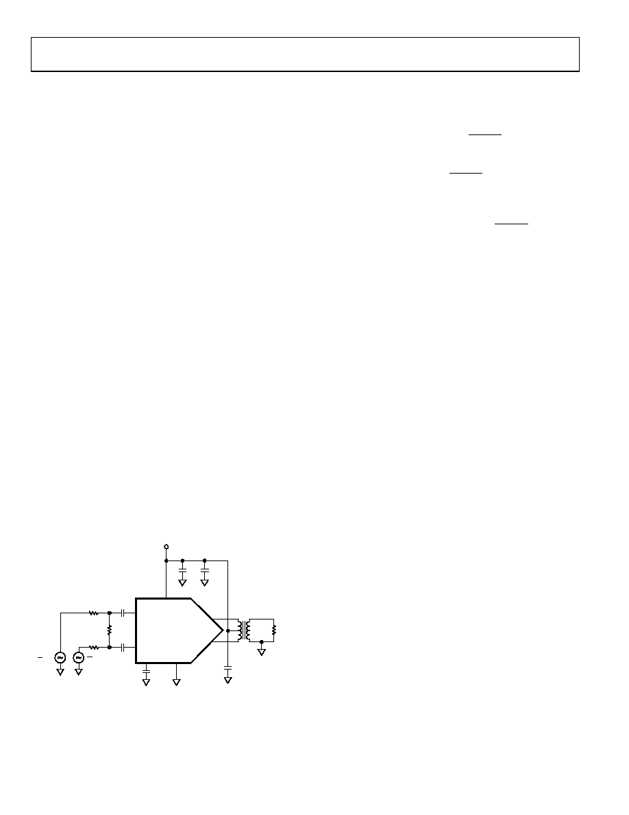
VIN+
VIN–
VCC
GND
AD8328
BYP
RL
5V
VIN
VOUT+
VOUT–
1
2
1
2
03
15
8-
0
19
Figure 19. Characterization Circuit
SPI PROGRAMMING AND GAIN ADJUSTMENT
The AD8328 is controlled through a serial peripheral interface
(SPI) of three digital data lines: CLK, DATEN, and SDATA.
Changing the gain requires eight bits of data to be streamed into
the SDATA port. The sequence of loading the SDATA register
begins on the falling edge of the DATEN pin, which activates
the CLK line. With the CLK line activated, data on the SDATA
line is clocked into the serial shift register on the rising edge of
the CLK pulses, MSB first. The 8-bit data-word is latched into
the attenuator core on the rising edge of the DATEN line. This
provides control over the changes in the output signal level. The
serial interface timing for the AD8328 is shown in Figure 3 and
Figure 4. The programmable gain range of the AD8328 is
28 dB to +31 dB with steps of 1 dB per least significant bit
(LSB). This provides a total gain range of 59 dB. The AD8328
was characterized with a differential signal on the input and a
TOKO 458PT-1087 2:1 transformer on the output. The AD8328
incorporates supply current scaling with gain code, as shown in
Figure 18. This allows reduced power consumption when
operating in lower gain codes.
INPUT BIAS, IMPEDANCE, AND TERMINATION
The VIN+ and VIN inputs have a dc bias level of VCC/2; therefore,
the input signal should be ac-coupled as shown in Figure 20.
The differential input impedance of the AD8328 is approximately
1.6 kΩ, while the single-ended input is 800 Ω. The high input
impedance of the AD8328 allows flexibility in termination and
properly matching filter networks. The AD8328 exhibits
optimum performance when driven with a pure differential
signal.
OUTPUT BIAS, IMPEDANCE, AND TERMINATION
The output stage of the AD8328 requires a bias of 5 V. The 5 V
power supply should be connected to the center tap of the
output transformer. In addition, the VCC applied to the center
tap of the transformer should be decoupled as seen in Figure 20.
相关PDF资料 |
PDF描述 |
|---|---|
| MAX11615EEE+ | IC ADC SERIAL 12BIT 8CH 16-QSOP |
| AD8328ACPZ | IC LINE DRIVE CABLE 5V 20-LFCSP |
| AD8321ARZ-REEL | IC LINE DVR CATV 20-SOIC T/R |
| MAX11614EEE+ | IC ADC SERIAL 12BIT 8CH 16-QSOP |
| MAX11210EEE+ | IC ADC 24BIT SPI/SRL 5SPS 16QSOP |
相关代理商/技术参数 |
参数描述 |
|---|---|
| AD8328ARQ-EVAL | 制造商:AD 制造商全称:Analog Devices 功能描述:5 V Upstream Cable Line Driver |
| AD8328ARQ-REEL | 制造商:Analog Devices 功能描述:SP Amp Line Driver Amp Single 5.25V 20-Pin QSOP T/R |
| AD8328ARQZ | 功能描述:IC LINE DRIVE CABLE 5V 20-QSOP RoHS:是 类别:集成电路 (IC) >> 线性 - 视频处理 系列:- 产品变化通告:Product Discontinuation 07/Mar/2011 标准包装:3,000 系列:OMNITUNE™ 类型:调谐器 应用:移动电话,手机,视频显示器 安装类型:表面贴装 封装/外壳:65-WFBGA 供应商设备封装:PG-WFSGA-65 包装:带卷 (TR) 其它名称:SP000365064 |
| AD8328ARQZ-REEL | 制造商:Analog Devices 功能描述:SP Amp Line Driver Amp Single 5.25V 20-Pin QSOP T/R 制造商:Rochester Electronics LLC 功能描述:QSOP LOW COST +5V CABLE LINE DRIVER - Tape and Reel 制造商:Analog Devices 功能描述:IC,Digitally Controlled Gain Amplifier,SINGLE,SSOP,20PIN,PLASTIC |
| AD8330 | 制造商:AD 制造商全称:Analog Devices 功能描述:Low Cost, DC to 150 MHz Variable Gain Amplifier |
发布紧急采购,3分钟左右您将得到回复。