- 您现在的位置:买卖IC网 > PDF目录16924 > AD8330-EVALZ (Analog Devices Inc)BOARD EVAL FOR AD8330 PDF资料下载
参数资料
| 型号: | AD8330-EVALZ |
| 厂商: | Analog Devices Inc |
| 文件页数: | 18/32页 |
| 文件大小: | 0K |
| 描述: | BOARD EVAL FOR AD8330 |
| 标准包装: | 1 |
| 每 IC 通道数: | 1 - 单 |
| 放大器类型: | 可变增益 |
| 输出类型: | 差分,满摆幅 |
| 转换速率: | 1500 V/µs |
| -3db带宽: | 150MHz |
| 工作温度: | -40°C ~ 85°C |
| 电流供应(主 IC): | 20mA |
| 电压 - 电源,单路/双路(±): | 2.7 V ~ 6 V |
| 板类型: | 完全填充 |
| 已供物品: | 板 |
| 已用 IC / 零件: | AD8330 |
| 产品目录页面: | 775 (CN2011-ZH PDF) |
| 相关产品: | AD8330ACPZ-R7DKR-ND - IC AMP VGA 150MHZ LN LP 16LFCSP AD8330ACPZ-R2-ND - IC AMP VGA 150MHZ LN LP 16LFCSP AD8330ACPZ-RL-ND - IC AMP VGA 150MHZ LN LP 16LFCSP AD8330ACPZ-R7CT-ND - IC AMP VGA 150MHZ LN LP 16LFCSP AD8330ACPZ-R7TR-ND - IC AMP VGA 150MHZ LN LP 16LFCSP AD8330ARQZ-RL-ND - IC AMP VGA 150MHZ LN LP 16QSOP AD8330ARQZ-R7-ND - IC AMP VGA 150MHZ LN LP 16QSOP AD8330ARQZ-ND - IC AMP VGA 150MHZ LN LP 16QSOP |
第1页第2页第3页第4页第5页第6页第7页第8页第9页第10页第11页第12页第13页第14页第15页第16页第17页当前第18页第19页第20页第21页第22页第23页第24页第25页第26页第27页第28页第29页第30页第31页第32页
Data Sheet
AD8330
Rev. F | Page 25 of 32
APPLICATIONS INFORMATION
The versatility of the AD8330, its very constant ac response over
a wide range of gains, the large signal dynamic range, output
swing, single supply operation, and low power consumption
commend this VGA to a diverse variety of applications. Only a
few can be described here, including the most basic uses and some
unusual ones.
ADC DRIVING
The AD8330 is well-suited to drive a high speed converter.
There are many high speed converters available, but to illustrate
the general features, the example in this data sheet uses one of
the least expensive, the AD9214. This is available in three
grades for operation at 65 MHz, 80 MHz, and 105 MHz; the
AD9214BRS-80 is a good complement to the general capabili-
ties of this VGA.
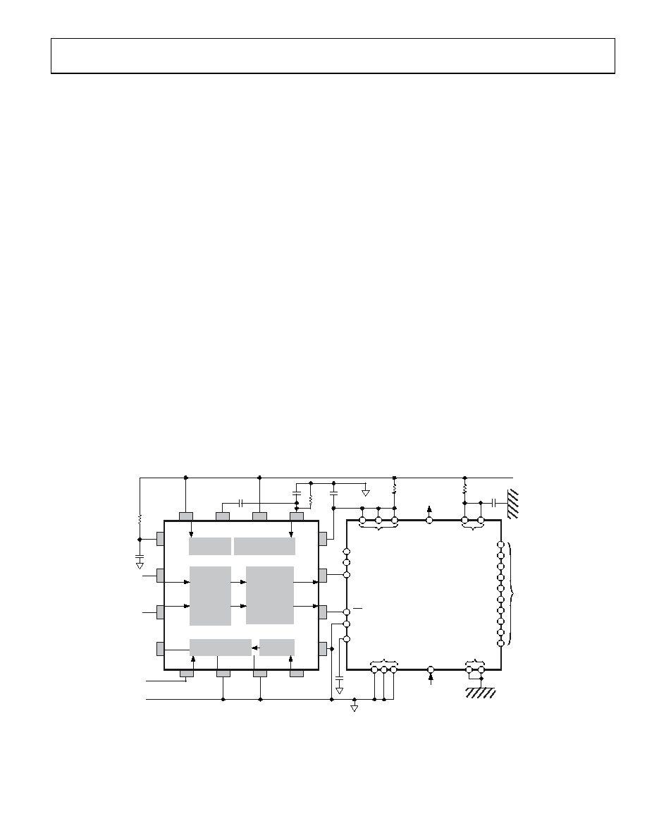
Figure 63 shows the connections to drive an ADC. A 3.3 V
supply is used for both parts. The ADC requires that its input
pins be positioned at one third of the supply, or 1.1 V. Given
that the default output level of the VGA is one-half the supply
or 1.65 V, a small correction is introduced by the 8 kΩ resistor
from CNTR to ground. The ADC specifications require that the
common-mode input be within ±0.2 V of the nominal 1.1 V;
variations of up to ±20% in the AD8330 on-chip resistors change
this voltage by only ±70 mV. With the connections shown in
Figure 63, the AD9214 is able to receive an input of 2 V p-p; the
peak output of the AD8330 can be reduced if desired by adding
a resistor
from VMAG to ground. An overrange condition is signaled by a
high state on Pin OR of the AD9214. DFS/GAIN is unconnected
in this example producing an offset-binary output. To provide a
twos complement output, it should be connected to the REF pin.
For ADCs running at sampling rates substantially below the
bandwidth of the AD8330, an intervening noise filter is
recommended to limit the noise bandwidth. A one-pole filter
can easily be created with a single differential capacitor between
the OPHI and OPLO outputs. For a corner frequency of fC, the
capacitor should have a value of
CFILT = 1/942 fC
(26)
For example, a 10 MHz corner requires about 100 pF.
SIMPLE AGC AMPLIFIER
Figure 64 illustrates the use of the inverted gain mode and the
offset gain range (0.2 V < VDBS < 1.7 V) in supporting a low cost
AGC loop. Q1 is used as a detector. When OPHI is sufficiently
higher than CNTR, due to the signal swing, it conducts and
charges C1. This raises VDBS and rapidly lowers the gain. Note
that MODE is grounded (see Figure 48). The minimum voltage
needed across R1 to set up the full gain is 0.2 V because CMGN
is dc open-circuited (this does not alter VMAG) and the maxi-
mum voltage is 1.7 V.
COMM
OPHI
INLO
OPLO
INHI
VPSI
VPSO
CMOP
MODE
VDBS
CMGN
OFST
CNTR
ENBL
VPOS
BIAS AND
V-REF
CM MODE AND
OFFSET CONTROL
OUTPUT
STAGES
OUTPUT
CONTROL
VGA CORE
AD9214BRS-80
DAT
A
O
UT
P
UT
S
D0
D1
D2
D3
D4
D5
D6
D7
D8
D9
DGND
CLK
AGND
CLOCK
REF
0.1F
REFSENSE
NC
ANALOG GROUND
AIN
DFS/GAIN
PWRDN
DIGITAL
GROUND
GAIN BIAS,
VDBS, 0V–1.5V
NC
INPUT,
±2V MAX
0.1F
10
GAIN INTERFACE
CHPF
8k
0.1F
AVDD
OR
DrVDD
3.3
OVER-
RANGE
3.3
0.1F
VS, 3.3V
03217-
064
VMAG
Figure 63. Driving an Analog-to-Digital Converter (Preliminary)
相关PDF资料 |
PDF描述 |
|---|---|
| 202D163-3-0 | BOOT MOLDED |
| RCC06DRTS-S93 | CONN EDGECARD 12POS DIP .100 SLD |
| VI-B5Z-EX | CONVERTER MOD DC/DC 2V 30W |
| 234A032-100-0 | BOOT MOLDED |
| LQW15AN1N5D00D | INDUCTOR 1.5NH 1000MA 0402 |
相关代理商/技术参数 |
参数描述 |
|---|---|
| AD8331 | 制造商:AD 制造商全称:Analog Devices 功能描述:Ultralow Noise VGAs with Preamplifier and Programmable RIN |
| AD8331_06 | 制造商:AD 制造商全称:Analog Devices 功能描述:Ultralow Noise VGAs with Preamplifier and Programmable RIN |
| AD8331_10 | 制造商:AD 制造商全称:Analog Devices 功能描述:Ultralow Noise VGAs with Preamplifier and Programmable RIN |
| AD8331ARQ | 功能描述:IC VGA SINGLE W/PREAMP 20-QSOP RoHS:否 类别:集成电路 (IC) >> 线性 - 放大器 - 专用 系列:X-AMP® 产品培训模块:Lead (SnPb) Finish for COTS Obsolescence Mitigation Program 标准包装:60 系列:- 类型:可变增益放大器 应用:CATV 安装类型:表面贴装 封装/外壳:20-WQFN 裸露焊盘 供应商设备封装:20-TQFN-EP(5x5) 包装:托盘 |
| AD8331ARQ-REEL | 功能描述:IC VGA SINGLE W/PREAMP 20-SSOP RoHS:否 类别:集成电路 (IC) >> 线性 - 放大器 - 专用 系列:X-AMP® 产品培训模块:Lead (SnPb) Finish for COTS Obsolescence Mitigation Program 标准包装:60 系列:- 类型:可变增益放大器 应用:CATV 安装类型:表面贴装 封装/外壳:20-WQFN 裸露焊盘 供应商设备封装:20-TQFN-EP(5x5) 包装:托盘 |
发布紧急采购,3分钟左右您将得到回复。