参数资料
| 型号: | AD8330ARQZ |
| 厂商: | Analog Devices Inc |
| 文件页数: | 1/32页 |
| 文件大小: | 0K |
| 描述: | IC AMP VGA 150MHZ LN LP 16QSOP |
| 标准包装: | 98 |
| 放大器类型: | 可变增益 |
| 电路数: | 1 |
| 输出类型: | 差分,满摆幅 |
| 转换速率: | 1500 V/µs |
| -3db带宽: | 150MHz |
| 电流 - 输入偏压: | 100nA |
| 电流 - 电源: | 20mA |
| 电压 - 电源,单路/双路(±): | 2.7 V ~ 6 V |
| 工作温度: | -40°C ~ 85°C |
| 安装类型: | 表面贴装 |
| 封装/外壳: | 16-SSOP(0.154",3.90mm 宽) |
| 供应商设备封装: | 16-QSOP |
| 包装: | 管件 |
| 产品目录页面: | 775 (CN2011-ZH PDF) |
| 配用: | AD8330-EVALZ-ND - BOARD EVAL FOR AD8330 |
当前第1页第2页第3页第4页第5页第6页第7页第8页第9页第10页第11页第12页第13页第14页第15页第16页第17页第18页第19页第20页第21页第22页第23页第24页第25页第26页第27页第28页第29页第30页第31页第32页
Low Cost, DC to 150 MHz
Variable Gain Amplifier
Data Sheet
Rev. F
Information furnished by Analog Devices is believed to be accurate and reliable. However, no
responsibilityisassumedbyAnalogDevicesforitsuse,norforanyinfringementsofpatentsorother
rightsofthirdpartiesthatmayresultfromitsuse.Specificationssubjecttochangewithoutnotice.No
license is granted by implication or otherwise under any patent or patent rights of Analog Devices.
Trademarksandregisteredtrademarksarethepropertyoftheirrespectiveowners.
One Technology Way, P.O. Box 9106, Norwood, MA 02062-9106, U.S.A.
Tel: 781.329.4700
2003–2012 Analog Devices, Inc. All rights reserved.
FEATURES
Fully differential signal path, also used
with single-sided signals
Inputs from 0.3 mV to 1 V rms, rail-to-rail outputs
Differential R
IN = 1 k; ROUT (each output) 75
Automatic offset compensation (optional)
Linear-in-dB and linear-in-magnitude gain modes
0 dB to 50 dB, for 0 V < V
DBS < 1.5 V (30 mV/dB)
Inverted gain mode: 50 dB to 0 dB at 30 mV/dB
×0.03 to ×10 nominal gain for 15 mV < V
MAG < 5 V
Constant bandwidth: 150 MHz at all gains
Low noise: 5 nV/√Hz typical at maximum gain
Low distortion: ≤62 dBc typical
Low power: 20 mA typical at V
S of 2.7 V to 6 V
Available in a space-saving, 3 mm × 3 mm LFCSP package
APPLICATIONS
Pre-ADC signal conditioning
75 cable driving adjust
AGC amplifiers
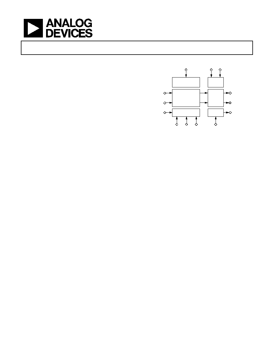
FUNCTIONAL BLOCK DIAGRAM
OPHI
CMOP
OPLO
VMAG
ENBL
BIAS AND VREF
VGA CORE
OUTPUT
CONTROL
GAIN INTERFACE
OUTPUT
STAGES
CM AND
OFFSET
CONTROL
OFST CNTR
INHI
INLO
MODE
VDBS
COMM
CMGN
03217-
101
Figure 1.
GENERAL DESCRIPTION
The AD8330 is a wideband variable gain amplifier for applications
requiring a fully differential signal path, low noise, well-defined
gain, and moderately low distortion, from dc to 150 MHz. The
input pins can also be driven from a single-ended source. The
peak differential input is ±2 V, allowing sine wave operation at
1 V rms with generous headroom. The output pins can drive
single-sided loads essentially rail-to-rail. The differential output
resistance is 150 . The output swing is a linear function of the
voltage applied to the VMAG pin that internally defaults to 0.5 V,
providing a peak output of ±2 V. This can be raised to 10 V p-p,
limited by the supply voltage.
The basic gain function is linear-in-dB, controlled by the voltage
applied to Pin VDBS. The gain ranges from 0 dB to 50 dB for
control voltages between 0 V and 1.5 V—a slope of 30 mV/dB.
The gain linearity is typically within ±0.1 dB. By changing the
logic level on Pin MODE, the gain decreases over the same range,
with an opposite slope. A second gain control port is provided at
the VMAG pin and allows the user to vary the numeric gain from
a factor of 0.03 to 10. All the parameters of the AD8330 have low
sensitivities to temperature and supply voltages.
Using VMAG, the basic 0 dB to 50 dB range can be reposi-
tioned to any value from 20 dB higher (that is, 20 dB to 70 dB)
to at least 30 dB lower (that is, –30 dB to +20 dB) to suit the
application, thereby providing an unprecedented gain range of
over 100 dB. A unique aspect of the AD8330 is that its bandwidth
and pulse response are essentially constant for all gains, over both
the basic 50 dB linear-in-dB range, but also when using the
linear-in-magnitude function. The exceptional stability of the
HF response over the gain range is of particular value in those
VGA applications where it is essential to maintain accurate gain
law-conformance at high frequencies.
An external capacitor at Pin OFST sets the high-pass corner of
an offset reduction loop, whose frequency can be as low as 5 Hz.
When this pin is grounded, the signal path becomes dc-coupled.
When used to drive an ADC, an external common-mode control
voltage at Pin CNTR can be driven to within 0.5 V of either ground
or VS to accommodate a wide variety of requirements. By default,
the two outputs are positioned at the midpoint of the supply, VS/2.
Other features, such as two levels of power-down (fully off and a
hibernate mode), further extend the practical value of this excep-
tionally versatile VGA.
The AD8330 is available in 16-lead LFCSP and 16-lead QSOP
packages and is specified for operation from 40°C to +85°C.
相关PDF资料 |
PDF描述 |
|---|---|
| LT1014CN#PBF | IC PRECISION OP-AMP QUAD 14-DIP |
| PEC06DADN | CONN HEADER .100 DUAL STR 12POS |
| AD8367ARUZ | IC AMP VGA 14TSSOP |
| LT1994MPDD#PBF | IC OP AMP I/O DIFF LN 8-DFN |
| PBC08SBCN | CONN HEADER .100 SINGL R/A 8POS |
相关代理商/技术参数 |
参数描述 |
|---|---|
| AD8330ARQZ-R7 | 功能描述:IC AMP VGA 150MHZ LN LP 16QSOP RoHS:是 类别:集成电路 (IC) >> Linear - Amplifiers - Instrumentation 系列:- 标准包装:50 系列:- 放大器类型:J-FET 电路数:2 输出类型:- 转换速率:3.5 V/µs 增益带宽积:1MHz -3db带宽:- 电流 - 输入偏压:30pA 电压 - 输入偏移:2000µV 电流 - 电源:200µA 电流 - 输出 / 通道:- 电压 - 电源,单路/双路(±):7 V ~ 36 V,±3.5 V ~ 18 V 工作温度:0°C ~ 70°C 安装类型:通孔 封装/外壳:8-DIP(0.300",7.62mm) 供应商设备封装:8-PDIP 包装:管件 |
| AD8330ARQZ-RL | 功能描述:IC AMP VGA 150MHZ LN LP 16QSOP RoHS:是 类别:集成电路 (IC) >> Linear - Amplifiers - Instrumentation 系列:- 标准包装:150 系列:- 放大器类型:音频 电路数:2 输出类型:- 转换速率:5 V/µs 增益带宽积:12MHz -3db带宽:- 电流 - 输入偏压:100nA 电压 - 输入偏移:500µV 电流 - 电源:6mA 电流 - 输出 / 通道:50mA 电压 - 电源,单路/双路(±):4 V ~ 32 V,±2 V ~ 16 V 工作温度:-40°C ~ 85°C 安装类型:表面贴装 封装/外壳:8-TSSOP(0.173",4.40mm 宽) 供应商设备封装:8-TSSOP 包装:管件 |
| AD8330-EVAL | 制造商:AD 制造商全称:Analog Devices 功能描述:Low Cost, DC to 150 MHz Variable Gain Amplifier |
| AD8330-EVALZ | 功能描述:BOARD EVAL FOR AD8330 RoHS:是 类别:编程器,开发系统 >> 评估板 - 运算放大器 系列:- 产品培训模块:Lead (SnPb) Finish for COTS Obsolescence Mitigation Program 标准包装:1 系列:- |
| AD8331 | 制造商:AD 制造商全称:Analog Devices 功能描述:Ultralow Noise VGAs with Preamplifier and Programmable RIN |
发布紧急采购,3分钟左右您将得到回复。