参数资料
| 型号: | AD8330ARQZ |
| 厂商: | Analog Devices Inc |
| 文件页数: | 8/32页 |
| 文件大小: | 0K |
| 描述: | IC AMP VGA 150MHZ LN LP 16QSOP |
| 标准包装: | 98 |
| 放大器类型: | 可变增益 |
| 电路数: | 1 |
| 输出类型: | 差分,满摆幅 |
| 转换速率: | 1500 V/µs |
| -3db带宽: | 150MHz |
| 电流 - 输入偏压: | 100nA |
| 电流 - 电源: | 20mA |
| 电压 - 电源,单路/双路(±): | 2.7 V ~ 6 V |
| 工作温度: | -40°C ~ 85°C |
| 安装类型: | 表面贴装 |
| 封装/外壳: | 16-SSOP(0.154",3.90mm 宽) |
| 供应商设备封装: | 16-QSOP |
| 包装: | 管件 |
| 产品目录页面: | 775 (CN2011-ZH PDF) |
| 配用: | AD8330-EVALZ-ND - BOARD EVAL FOR AD8330 |
第1页第2页第3页第4页第5页第6页第7页当前第8页第9页第10页第11页第12页第13页第14页第15页第16页第17页第18页第19页第20页第21页第22页第23页第24页第25页第26页第27页第28页第29页第30页第31页第32页
AD8330
Data Sheet
Rev. F | Page 16 of 32
Alternatively, this can be expressed as a numerical gain
magnitude
V
BN
DBS
G
6
.
0
10
=
(2)
The gain can be increased or decreased by changing the voltage,
VMAG, applied to the VMAG pin. The internally set default value
of 500 mV is derived from the same band gap reference that
determines the decibel scaling. The tolerance on this voltage,
and mismatches in certain on-chip resistors, cause small gain
errors (see the Specifications section). Though not all appli-
cations of VGAs demand accurate gain calibration, it is a
valuable asset in many situations, for example, in reducing
design tolerances.
Figure 47 shows the core circuit in more detail. The range and
scaling of VDBS is independent of the supply voltage, and the
gain control pin, VDBS, presents a high incremental input re-
sistance (~100 MΩ) with a low bias current (~100 nA), making
the AD8330 easy to drive from a variety of gain control sources.
Inversion of the Gain Slope
The AD8330 supports many features that further extend the
versatility of this VGA in wide bandwidth gain control systems.
For example, the logic pin, MODE, allows the slope of the gain
function to be inverted, so that the basic gain starts at +50 dB
for a gain voltage, VDBS, of zero and runs down to 0 dB when
this voltage is at its maximum specified value of 1.5 V. The basic
forms of these two gain control modes are shown in Figure 48.
0.25
10
20
VDBS (V)
G
AI
N
(
d
B)
0
30
40
50
0
0.50
0.75
1.0
1.25
1.50
MODE PIN
LOW, GAIN
DECREASES
WITH VDBS
MODE PIN
HIGH, GAIN
INCREASES
WITH VDBS
03217-
049
Figure 48. Two Gain Directions of the AD8330
Gain Magnitude Control (VMAG)
In addition to the basic linear-in-dB control, two more gain
control features are provided. The voltage applied to Pin VMAG
provides accurate linear-in-magnitude gain control with a very
rapid response. The bandwidth of this interface is >100 MHz.
When this pin is unconnected, VMAG assumes its default value of
500 mV (see Figure 47) to set up the basic 0 dB to 50 dB range.
However, any voltage from ~15 mV to 5 V can be applied either
to lower the gain by up to 30 dB or to raise it by 20 dB. The
combined gain span is thus 100 dB, that is, the 50 dB basic gain
span provided by VDBS plus a 60 dB linear-in-magnitude span
provided by VMAG. The latter modifies the basic numerical gain
GBN to generate a total gain, expressed here in magnitude terms.
V
5
.
0
MAG
BN
T
V
G
G =
(3)
Using this to calculate the output voltage,
VOUT = 2 × GIN × VIN × VMAG
(4)
from which it is apparent that the AD8330 implements a linear,
two-quadrant multiplier with a bipolar VIN and a unipolar VMAG.
Because the AD8330 is a dc-coupled system, it can be used in
many applications where a wideband two-quadrant multiplier
function is required, from dc up to about 100 MHz from either
input (VIN or VMAG).
As VMAG is varied, so also is the peak output magnitude, up to a
point where this is limited by the absolute output limit imposed
by the supply voltage. In the absence of the latter effect, the
peak output into an open-circuited load is just
VOUT_PK = ±4 VMAG
(5)
whereas for a load resistance of RL directly across OPHI and
OPLO, it is
(
)
150
2
_
+
±
=
L
MAG
PK
OUT
R
V
(6)
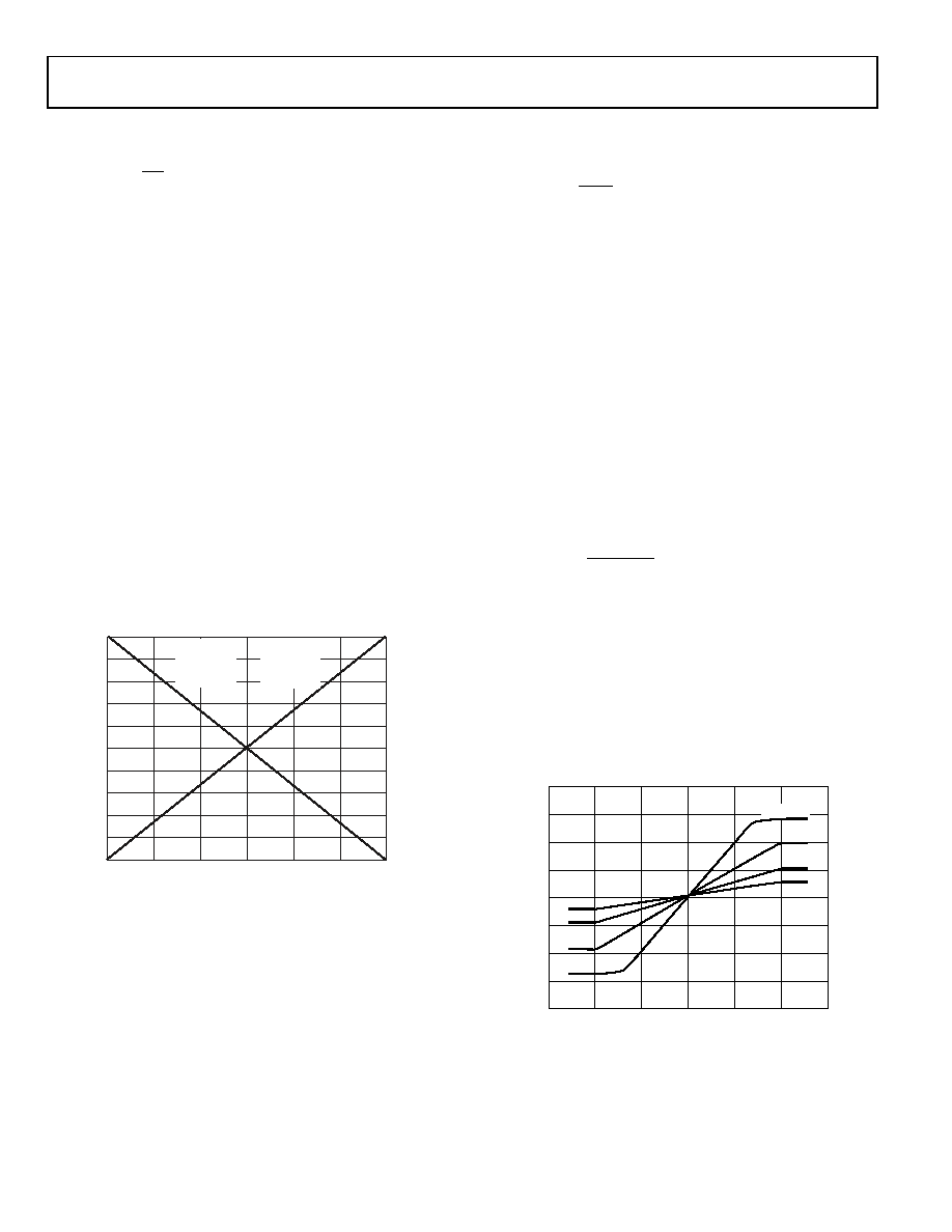
RL = O/C, VDBS = 0 V, VIN is swept from 2.5 V dc to +2.5 V dc, and
VMAG is set to 0.25 V, 0.5 V, 1 V, and 2 V. Except for the last value
of VMAG, the peak output follows Equation 5. This exceeds the
supply-limited value when VMAG = 2 V and the peak output is
±5.65 V, that is, ±6 V 0.35 V. Figure 50 demonstrates the high
speed multiplication capability. The signal input is a 100 MHz,
0.1 V sine wave, VDBS is set to 0.6 V, and VMAG is a square wave at
5 MHz alternating from 0.25 V to 1 V. The output is ideally a
sine wave switching in amplitude between 0.5 V and 2 V.
VIN ( V)
8
3
1
2
–
3
–
V
O
UT
(V)
4
0
–4
–8
–1
6
2
–2
–6
0
2
VMAG = 2V
1V
0.5V
0.25V
03217-
050
Figure 49. Effect of VMAG on Gain and Peak Output
相关PDF资料 |
PDF描述 |
|---|---|
| LT1014CN#PBF | IC PRECISION OP-AMP QUAD 14-DIP |
| PEC06DADN | CONN HEADER .100 DUAL STR 12POS |
| AD8367ARUZ | IC AMP VGA 14TSSOP |
| LT1994MPDD#PBF | IC OP AMP I/O DIFF LN 8-DFN |
| PBC08SBCN | CONN HEADER .100 SINGL R/A 8POS |
相关代理商/技术参数 |
参数描述 |
|---|---|
| AD8330ARQZ-R7 | 功能描述:IC AMP VGA 150MHZ LN LP 16QSOP RoHS:是 类别:集成电路 (IC) >> Linear - Amplifiers - Instrumentation 系列:- 标准包装:50 系列:- 放大器类型:J-FET 电路数:2 输出类型:- 转换速率:3.5 V/µs 增益带宽积:1MHz -3db带宽:- 电流 - 输入偏压:30pA 电压 - 输入偏移:2000µV 电流 - 电源:200µA 电流 - 输出 / 通道:- 电压 - 电源,单路/双路(±):7 V ~ 36 V,±3.5 V ~ 18 V 工作温度:0°C ~ 70°C 安装类型:通孔 封装/外壳:8-DIP(0.300",7.62mm) 供应商设备封装:8-PDIP 包装:管件 |
| AD8330ARQZ-RL | 功能描述:IC AMP VGA 150MHZ LN LP 16QSOP RoHS:是 类别:集成电路 (IC) >> Linear - Amplifiers - Instrumentation 系列:- 标准包装:150 系列:- 放大器类型:音频 电路数:2 输出类型:- 转换速率:5 V/µs 增益带宽积:12MHz -3db带宽:- 电流 - 输入偏压:100nA 电压 - 输入偏移:500µV 电流 - 电源:6mA 电流 - 输出 / 通道:50mA 电压 - 电源,单路/双路(±):4 V ~ 32 V,±2 V ~ 16 V 工作温度:-40°C ~ 85°C 安装类型:表面贴装 封装/外壳:8-TSSOP(0.173",4.40mm 宽) 供应商设备封装:8-TSSOP 包装:管件 |
| AD8330-EVAL | 制造商:AD 制造商全称:Analog Devices 功能描述:Low Cost, DC to 150 MHz Variable Gain Amplifier |
| AD8330-EVALZ | 功能描述:BOARD EVAL FOR AD8330 RoHS:是 类别:编程器,开发系统 >> 评估板 - 运算放大器 系列:- 产品培训模块:Lead (SnPb) Finish for COTS Obsolescence Mitigation Program 标准包装:1 系列:- |
| AD8331 | 制造商:AD 制造商全称:Analog Devices 功能描述:Ultralow Noise VGAs with Preamplifier and Programmable RIN |
发布紧急采购,3分钟左右您将得到回复。