参数资料
| 型号: | AD8332ARUZ-RL |
| 厂商: | Analog Devices Inc |
| 文件页数: | 18/56页 |
| 文件大小: | 0K |
| 描述: | IC AMP VAR GAIN 2CHAN 28TSSOP |
| 标准包装: | 2,500 |
| 系列: | X-AMP® |
| 类型: | 可变增益放大器 |
| 应用: | 信号处理 |
| 安装类型: | 表面贴装 |
| 封装/外壳: | 28-TSSOP(0.173",4.40mm 宽) |
| 供应商设备封装: | 28-TSSOP |
| 包装: | 带卷 (TR) |
| 配用: | AD8332-EVALZ-ND - BOARD EVAL FOR AD8332 |
第1页第2页第3页第4页第5页第6页第7页第8页第9页第10页第11页第12页第13页第14页第15页第16页第17页当前第18页第19页第20页第21页第22页第23页第24页第25页第26页第27页第28页第29页第30页第31页第32页第33页第34页第35页第36页第37页第38页第39页第40页第41页第42页第43页第44页第45页第46页第47页第48页第49页第50页第51页第52页第53页第54页第55页第56页
AD8331/AD8332/AD8334
Rev. G | Page 25 of 56
The linear-in-dB, gain control interface is trimmed for slope and
absolute accuracy. The gain range is +48 dB, extending from
4.5 dB to +43.5 dB in LO gain and +7.5 dB to +55.5 dB in HI
gain mode. The slope of the gain control interface is 50 dB/V,
and the gain control range is 40 mV to 1 V. Equation 1 and
Equation 2 are the expressions for gain.
GAIN (dB) = 50 (dB/V) × VGAIN 6.5 dB, (HILO = LO)
(1)
or
GAIN (dB) = 50 (dB/V) × VGAIN + 5.5 dB, (HILO = HI)
(2)
The ideal gain characteristics are shown in Figure 73.
60
50
40
30
20
10
0
–10
0
0.2
0.4
0.6
0.8
1.0
1.1
GA
IN
(
d
B
)
VGAIN (V)
03
19
9-
0
73
HILO = HI
HILO = LO
ASCENDING GAIN MODE
DESCENDING GAIN MODE
(WHERE AVAILABLE)
Figure 73. Ideal Gain Control Characteristics
The gain slope is negative with MODE pulled high (where
available), as follows:
GAIN (dB) = 50 (dB/V) × VGAIN + 45.5 dB, (HILO = LO)
(3)
or
GAIN (dB) = 50 (dB/V) × VGAIN + 57.5 dB, (HILO = HI)
(4)
The LNA converts a single-ended input to a differential output
with a voltage gain of 19 dB. If only one output is used, the gain
is 13 dB. The inverting output is used for active input impedance
termination. Each of the LNA outputs is capacitively coupled to
a VGA input. The VGA consists of an attenuator with a range of
48 dB followed by an amplifier with 21 dB of gain for a net gain
range of 27 dB to +21 dB. The X-AMP, gain interpolation
technique results in low gain error and uniform bandwidth, and
differential signal paths minimize distortion.
The final stage is a logic programmable amplifier with gains of
3.5 dB or 15.5 dB. The LO and HI gain modes are optimized for
12-bit and 10-bit ADC applications, in terms of output-referred
noise and absolute gain range. Output voltage limiting can be
programmed by the user.
LOW NOISE AMPLIFIER (LNA)
relies on a proprietary ultralow noise preamplifier at the beginning
of the signal chain, which minimizes the noise contribution in the
following VGA. Active impedance control optimizes noise per-
formance for applications that benefit from input matching.
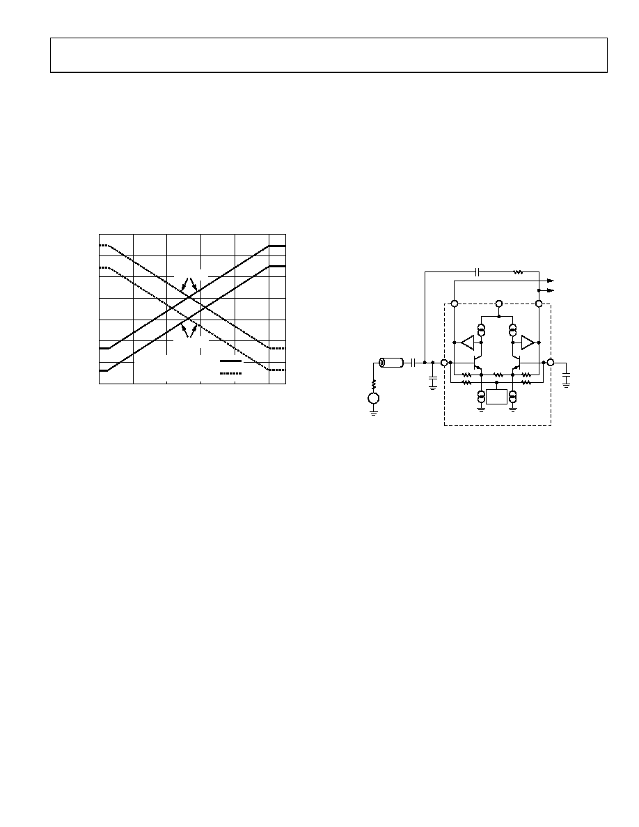
A simplified schematic of the LNA is shown in Figure 74. INH
is capacitively coupled to the source. A bias generator establishes dc
input bias voltages of 3.25 V and centers the output common-
mode levels at 2.5 V. A capacitor CLMD (can be the same value as
the input coupling capacitor CINH) is connected from the LMD
pin to ground to decouple the LMD bus. The LMD pin is not
useable for configuring the LNA as a differential input amplifier.
03
199
-07
4
RS
CINH
CSH
I0
Q1
Q2
VPOS
VCM
BIAS
LOP
INH
3.25V
–a
LON
TO
VGA
2.5V
CLMD
LMD
CIZ
RIZ
60
40
80
Figure 74. Simplified LNA Schematic
The LNA supports differential output voltages as high as 5 V p-p,
with positive and negative excursions of ±1.25 V, about a
common-mode voltage of 2.5 V. Because the differential gain
magnitude is 9, the maximum input signal before saturation is
±275 mV or +550 mV p-p. Overload protection ensures quick
recovery time from large input voltages. Because the inputs are
capacitively coupled to a bias voltage near midsupply, very large
inputs can be handled without interacting with the ESD protection.
Low value feedback resistors and the current-driving capability
of the output stage allow the LNA to achieve a low input-referred
voltage noise of 0.74 nV/√Hz. This is achieved with a current
consumption of only 11 mA per channel (55 mW). On-chip
resistor matching results in precise single-ended gains of 4.5×
(9× differential), critical for accurate impedance control. The use
of a fully differential topology and negative feedback minimizes
distortion. Low HD2 is particularly important in second harmonic
ultrasound imaging applications. Differential signaling enables
smaller swings at each output, further reducing third-order
distortion.
相关PDF资料 |
PDF描述 |
|---|---|
| AD5328ARU | IC DAC 12BIT OCTAL W/BUF 16TSSOP |
| AD8332ACPZ-RL | IC AMP VAR GAIN 2CHAN 32LFCSP |
| SY88883VKG | IC POST AMP CML LP LIMIT 10-MSOP |
| VE-252-IV-F4 | CONVERTER MOD DC/DC 15V 150W |
| VE-22T-MY-B1 | CONVERTER MOD DC/DC 6.5V 50W |
相关代理商/技术参数 |
参数描述 |
|---|---|
| AD8332-EVAL | 制造商:Analog Devices 功能描述:DUAL VGA - Bulk |
| AD8332-EVALZ | 功能描述:BOARD EVAL FOR AD8332 RoHS:是 类别:编程器,开发系统 >> 评估板 - 运算放大器 系列:X-AMP® 产品培训模块:Lead (SnPb) Finish for COTS Obsolescence Mitigation Program 标准包装:1 系列:- |
| AD8333 | 制造商:AD 制造商全称:Analog Devices 功能描述:DC to 50 MHz, Dual I/Q Demodulator and Phase Shifter |
| AD8333ACPZ | 制造商:Analog Devices 功能描述:I/Q DEMODULATOR DUAL LFCSP-32 制造商:Analog Devices 功能描述:I/Q, DEMODULATOR, DUAL, LFCSP-32 |
| AD8333ACPZ-REEL | 功能描述:IC DEMODULATOR DUAL I/Q 32LFCSP RoHS:是 类别:RF/IF 和 RFID >> RF 解调器 系列:- 产品培训模块:Lead (SnPb) Finish for COTS Obsolescence Mitigation Program 标准包装:2,500 系列:- 功能:解调器 LO 频率:- RF 频率:70MHz ~ 300MHz P1dB:-9dBm 增益:- 噪音数据:6.36dB 电流 - 电源:41.5mA 电源电压:2.7 V 封装/外壳:28-WFQFN 裸露焊盘 供应商设备封装:28-TQFN-EP(5x5) 包装:带卷 (TR) |
发布紧急采购,3分钟左右您将得到回复。