参数资料
| 型号: | AD8332ARUZ-RL |
| 厂商: | Analog Devices Inc |
| 文件页数: | 38/56页 |
| 文件大小: | 0K |
| 描述: | IC AMP VAR GAIN 2CHAN 28TSSOP |
| 标准包装: | 2,500 |
| 系列: | X-AMP® |
| 类型: | 可变增益放大器 |
| 应用: | 信号处理 |
| 安装类型: | 表面贴装 |
| 封装/外壳: | 28-TSSOP(0.173",4.40mm 宽) |
| 供应商设备封装: | 28-TSSOP |
| 包装: | 带卷 (TR) |
| 配用: | AD8332-EVALZ-ND - BOARD EVAL FOR AD8332 |
第1页第2页第3页第4页第5页第6页第7页第8页第9页第10页第11页第12页第13页第14页第15页第16页第17页第18页第19页第20页第21页第22页第23页第24页第25页第26页第27页第28页第29页第30页第31页第32页第33页第34页第35页第36页第37页当前第38页第39页第40页第41页第42页第43页第44页第45页第46页第47页第48页第49页第50页第51页第52页第53页第54页第55页第56页
AD8331/AD8332/AD8334
Rev. G | Page 43 of 56
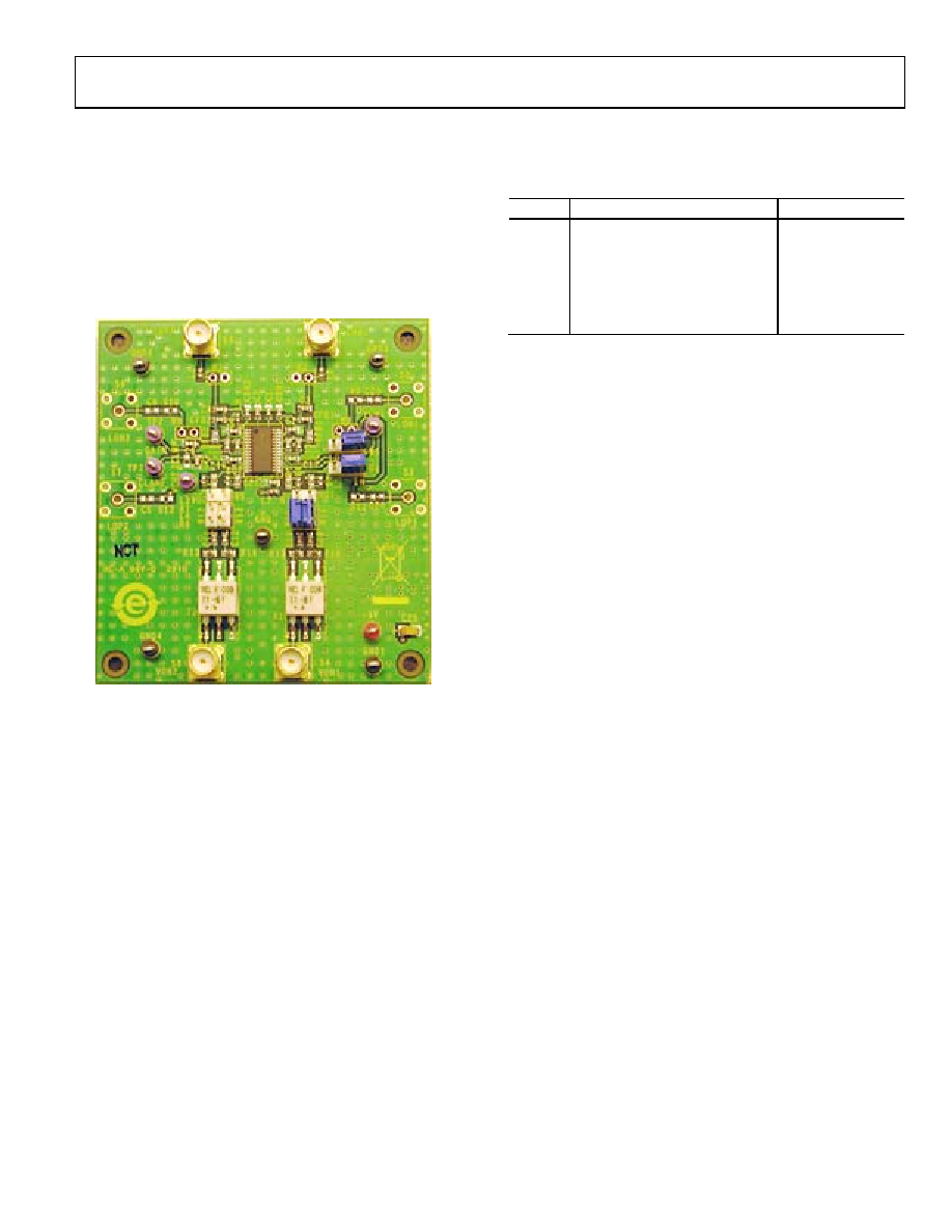
AD8332 EVALUATION BOARD
GENERAL DESCRIPTION
The AD8332-EVALZ is a platform for the testing and evaluation of
the AD8332 variable gain amplifier (VGA). The board is shipped
assembled and tested, and users need only connect the signal
and VGAIN sources to a single 5 V power supply. Figure 104 is a
photograph of the component side of the board, and Figure 105
shows the schematic. The AD8332-EVALZ is lead free and
RoHS compliant.
03
19
9-
13
1
Figure 104.Photograph of the AD8332-EVALZ
USER-SUPPLIED OPTIONAL COMPONENTS
The board is built and tested using the components shown in
black in Figure 105. Provisions are made for optional components
(shown in gray) that can be installed for testing at user discretion.
The default LNA input impedance is 50 Ω to match various
signal generators and network analyzers. Input impedances up to
6 kΩ are realized by changing the values of RFBx and CSHx. For
reference, Table 11 lists the common input impedance values
and corresponding adjustments. The board is designed for 0603
size, surface-mount components.
Table 11. LNA External Component Values for Common
Source Impedances
RIN (Ω)
RFB1, RFB2 (Ω Std 1% Value)
CSH1, CSH2 (pF)
50
274
22
75
412
12
100
562
8
200
1.13 k
1.2
500
3.01 k
None
6 k
∞
None
SMA connectors, S2, S3, S6, and S7, are provided for access to
the LNA outputs or the VGA inputs. If the LNA is used alone,
0.1 μF coupling capacitors can be installed at the C5, C9, C23,
and C24 locations. Resistors of 68 Ω to 100 Ω may be required
if the load capacitances, as seen by the LNA outputs, are larger
than approximately 10 pF.
A resistor can be inserted at RCLMP if output clamping is desired.
The peak-to-peak clamping level is adjusted by installing one of
the standard 1% resistor values listed in Table 8.
A high frequency differential probe connected to the 2-pin headers,
VOx, is the preferred method to observe a waveform at the VGA
output. A typical setup is shown in Figure 106. Single-ended loads
can be connected directly via the board edge SMA connectors.
Note that the AD8332 output amplifier is buffered with 237 Ω
resistors; therefore, be sure to compensate for attenuation if low
impedances are connected to the output SMAs.
MEASUREMENT SETUP
The basic board connections for measuring bandwidth are
shown in Figure 106. A 5 V, 100 mA (minimum) power supply
is required, and a low noise voltage reference supply is required
for VGAIN.
BOARD LAYOUT
The evaluation board circuitry uses four conductor layers.
The two inner layers are power and ground planes, and all
interconnecting circuitry is located on the outer layers. Figure 108
to Figure 111 illustrate the copper patterns.
相关PDF资料 |
PDF描述 |
|---|---|
| AD5328ARU | IC DAC 12BIT OCTAL W/BUF 16TSSOP |
| AD8332ACPZ-RL | IC AMP VAR GAIN 2CHAN 32LFCSP |
| SY88883VKG | IC POST AMP CML LP LIMIT 10-MSOP |
| VE-252-IV-F4 | CONVERTER MOD DC/DC 15V 150W |
| VE-22T-MY-B1 | CONVERTER MOD DC/DC 6.5V 50W |
相关代理商/技术参数 |
参数描述 |
|---|---|
| AD8332-EVAL | 制造商:Analog Devices 功能描述:DUAL VGA - Bulk |
| AD8332-EVALZ | 功能描述:BOARD EVAL FOR AD8332 RoHS:是 类别:编程器,开发系统 >> 评估板 - 运算放大器 系列:X-AMP® 产品培训模块:Lead (SnPb) Finish for COTS Obsolescence Mitigation Program 标准包装:1 系列:- |
| AD8333 | 制造商:AD 制造商全称:Analog Devices 功能描述:DC to 50 MHz, Dual I/Q Demodulator and Phase Shifter |
| AD8333ACPZ | 制造商:Analog Devices 功能描述:I/Q DEMODULATOR DUAL LFCSP-32 制造商:Analog Devices 功能描述:I/Q, DEMODULATOR, DUAL, LFCSP-32 |
| AD8333ACPZ-REEL | 功能描述:IC DEMODULATOR DUAL I/Q 32LFCSP RoHS:是 类别:RF/IF 和 RFID >> RF 解调器 系列:- 产品培训模块:Lead (SnPb) Finish for COTS Obsolescence Mitigation Program 标准包装:2,500 系列:- 功能:解调器 LO 频率:- RF 频率:70MHz ~ 300MHz P1dB:-9dBm 增益:- 噪音数据:6.36dB 电流 - 电源:41.5mA 电源电压:2.7 V 封装/外壳:28-WFQFN 裸露焊盘 供应商设备封装:28-TQFN-EP(5x5) 包装:带卷 (TR) |
发布紧急采购,3分钟左右您将得到回复。