- 您现在的位置:买卖IC网 > PDF目录68990 > AD8339ACPZ-R7 (ANALOG DEVICES INC) 0 MHz - 50 MHz RF/MICROWAVE I/Q DEMODULATOR PDF资料下载
参数资料
| 型号: | AD8339ACPZ-R7 |
| 厂商: | ANALOG DEVICES INC |
| 元件分类: | 调制器/解调器 |
| 英文描述: | 0 MHz - 50 MHz RF/MICROWAVE I/Q DEMODULATOR |
| 封装: | 6 X 6 MM, ROHS COMPLIANT, MO-220-VJJD-2, LFCSP-40 |
| 文件页数: | 33/36页 |
| 文件大小: | 2970K |
| 代理商: | AD8339ACPZ-R7 |
第1页第2页第3页第4页第5页第6页第7页第8页第9页第10页第11页第12页第13页第14页第15页第16页第17页第18页第19页第20页第21页第22页第23页第24页第25页第26页第27页第28页第29页第30页第31页第32页当前第33页第34页第35页第36页
AD8339
Rev. A | Page 6 of
36
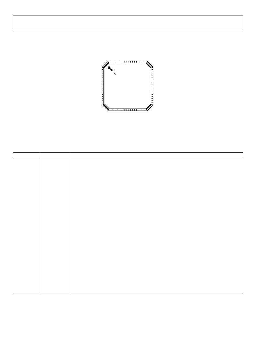
PIN CONFIGURATION AND FUNCTION DESCRIPTIONS
06
58
7-
0
02
8
7
6
5
1
4
3
229
30
31
32
28
34 33
27
14
13
17
12
11
18
15 16
20
37
35
19
21
22
23
24
PIN 1
INDICATOR
AD8339
TOP VIEW
(Not to Scale)
10
9
38
39
36
40
25
26
RF2N
RF2P
SCLK
CSB
COMM
VPOS
RF3P
RF3N
RS
T
S
SD
I
CO
M
VP
O
S
RF
1
P
RF
1N
RS
E
T
I1
O
P
Q1
O
P
VN
E
G
VP
O
S
SD
O
CO
M
VP
O
S
RF
4
P
RF
4N
LO
D
C
I4
O
P
Q4
O
P
VN
E
G
Q2OP
I2OP
4LOP
4LON
VPOS
VNEG
I3OP
Q3OP
NOTES
1. THE EXPOSED PAD IS NOT CONNECTED INTERNALLY. FOR
INCREASED RELIABILITY OF THE SOLDER JOINTS AND MAXIMUM
THERMAL CAPABILITY, IT IS RECOMMENDED THAT THE PAD BE
SOLDERED TO THE GROUND PLANE.
Figure 2. Pin Configuration
Table 3. Pin Function Descriptions
Pin No.
Mnemonic
Description
1, 2, 9, 10, 13,
14, 37, 38
RF1P to RF4P,
RF1N to RF4N
RF Inputs. Require external 2.5 V bias for optimum symmetrical input differential swing if
±5 V supplies
are used.
3, 4, 15, 36
COMM
Ground.
5
SCLK
Serial Interface Clock.
6
CSB
Serial Interface Chip Select Bar. Active low.
7, 8, 11, 16,
27, 28, 35
VPOS
Positive Supply. These pins should be decoupled with a ferrite bead in series with the supply and a
0.1 μF capacitor between the VPOS pins and ground. Because the VPOS pins are internally connected,
one set of supply decoupling components on each side of the chip should be sufficient.
12
SDO
Serial Interface Data Output. Normally connected to the SDI pin of the next chip or left open.
17
LODC
Decoupling Pin for LO. A 0.1 μF capacitor should be connected between this pin and ground. The value
of this capacitor affects the chip enable/disable times.
18, 19, 21, 22,
29, 30, 32, 33
I1OP to I4OP,
Q1OP to Q4OP
I/Q Outputs. These outputs provide a bidirectional current that can be converted back to a voltage via a
transimpedance amplifier. Multiple outputs can be summed by simply connecting them (wire-OR). The
bias voltage should be set to 0 V or less by the transimpedance amplifier (see Figure 53).
20, 23, 24, 31
VNEG
Negative Supply. These pins should be decoupled with a ferrite bead in series with the supply and a
0.1 μF capacitor between the VNEG pins and ground. Because the VNEG pins are internally connected,
one set of supply decoupling components for the chip should be sufficient.
25, 26
4LON, 4LOP
LO Inputs. No internal bias; optimally biased by an LVDS driver. For best performance, these inputs
should be driven differentially. If driven by a single-ended sine wave at 4LOP or 4LON, the signal level
should be >0 dBm (50 Ω) with external bias resistors.
34
RSET
Reset for LO Interface. Logic threshold is at ~1.3 V and therefore can be driven by >1.8 V CMOS logic.
39
SDI
Serial Interface Data Input. Logic threshold is at ~1.3 V and therefore can be driven by >1.8 V CMOS
logic.
40
RSTS
Reset for SPI Interface. Logic threshold is at ~1.5 V with ±0.3 V hysteresis and should be driven by >3.3 V
CMOS logic. For quick testing without the need to program the SPI, the voltage on the RSTS pin should
be pulled to 1.4 V; this enables all four channels in the phase (I = 1, Q = 0) state.
EP
Exposed Pad. The exposed pad is not connected internally. For increased reliability of the solder joints
and maximum thermal capability, it is recommended that the pad be soldered to the ground plane.
相关PDF资料 |
PDF描述 |
|---|---|
| AD8339ACPZ-RL | 0 MHz - 50 MHz RF/MICROWAVE I/Q DEMODULATOR |
| AD8339ACPZ | 0 MHz - 50 MHz RF/MICROWAVE I/Q DEMODULATOR |
| ADL5374ACPZ-WP | 3000 MHz - 4000 MHz RF/MICROWAVE QUADRAPHASE MODULATOR |
| ADL5375-05ACPZ-R7 | 400 MHz - 6000 MHz RF/MICROWAVE I/Q MODULATOR |
| AH212-S8G | 1800 MHz - 2400 MHz RF/MICROWAVE NARROW BAND MEDIUM POWER AMPLIFIER |
相关代理商/技术参数 |
参数描述 |
|---|---|
| AD8339ACPZ-RL | 功能描述:IC DEMODULATOR I/Q QUAD 40LFCSP RoHS:是 类别:RF/IF 和 RFID >> RF 解调器 系列:- 产品培训模块:Lead (SnPb) Finish for COTS Obsolescence Mitigation Program 标准包装:2,500 系列:- 功能:解调器 LO 频率:- RF 频率:70MHz ~ 300MHz P1dB:-9dBm 增益:- 噪音数据:6.36dB 电流 - 电源:41.5mA 电源电压:2.7 V 封装/外壳:28-WFQFN 裸露焊盘 供应商设备封装:28-TQFN-EP(5x5) 包装:带卷 (TR) |
| AD8339-EVALZ | 功能描述:BOARD EVAL AD8339 I/Q DEMOD RoHS:是 类别:RF/IF 和 RFID >> RF 评估和开发套件,板 系列:- 标准包装:1 系列:- 类型:GPS 接收器 频率:1575MHz 适用于相关产品:- 已供物品:模块 其它名称:SER3796 |
| AD834 | 制造商:AD 制造商全称:Analog Devices 功能描述:500 MHz Four-Quadrant Multiplier |
| AD834_12 | 制造商:AD 制造商全称:Analog Devices 功能描述:500 MHz Four-Quadrant Multiplier |
| AD8340 | 制造商:AD 制造商全称:Analog Devices 功能描述:400 MHz to 6 GHz Broadband Quadrature Modulator |
发布紧急采购,3分钟左右您将得到回复。