- 您现在的位置:买卖IC网 > PDF目录373944 > AD8341ACPZ-REEL72 (Analog Devices, Inc.) 1.5 GHz to 2.4 GHz RF Vector Modulator PDF资料下载
参数资料
| 型号: | AD8341ACPZ-REEL72 |
| 厂商: | Analog Devices, Inc. |
| 元件分类: | 调制器/解调器 |
| 英文描述: | 1.5 GHz to 2.4 GHz RF Vector Modulator |
| 中文描述: | 1.5 GHz至2.4 GHz射频矢量调制器 |
| 文件页数: | 13/20页 |
| 文件大小: | 556K |
| 代理商: | AD8341ACPZ-REEL72 |
AD8341
RF OUTPUT AND MATCHING
The RF outputs of the AD8341, RFOP, and RFOM, are open
collectors of a transimpedance amplifier which need to be
pulled up to the positive supply, preferably with RF chokes as
shown in Figure 31. The nominal output impedance looking
into each individual output pin is 25 . Consequently, the
differential output impedance is 50 .
Rev. 0 | Page 13 of 20
0
50
DIFFERENTIAL
100pF
1:1
RF
OUTPUT
RFOM
RFOP
R
T
R
T
120nH
100pF
V
P
G
M
±I
SIG
Figure 31. RF Output Interface to the AD8341 Showing
Coupling Capacitors, Pull-Up RF Chokes, and Balun
Since the output dc levels are at the positive supply, ac coupling
capacitors will usually be needed between the AD8341 outputs
and the next stage in the system.
A 1:1 RF broadband output balun, such as the ETC1-1-13
(M/A-COM), converts the differential output of the AD8341
into a single-ended signal. Note that the loss and balance of the
balun directly impact the apparent output power, noise floor,
and gain/phase errors of the AD8341. In critical applications,
narrow-band baluns with low loss and superior balance are
recommended.
If the output is taken in a single-ended fashion directly into a
50 load through a coupling capacitor, there will be an imped-
ance mismatch. This can be resolved with a 1:2 balun to convert
the single-ended 25 output impedance to 50 . If loss of
signal swing is not critical, a 25 back termination in series
with the output pin can also be used. The unused output pin
must still be pulled up to the positive supply. The user may load
it through a coupling capacitor with a dummy load to preserve
balance. The gain of the AD8341 when the output is single-
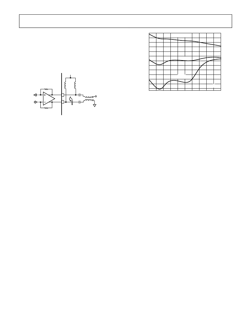
ended varies slightly with dummy load value as shown in Figure 32.
0
FREQUENCY (GHz)
–2.5
–3.0
–3.5
–4.0
–4.5
–5.0
–5.5
–6.0
–6.5
–7.0
–7.5
–8.0
–8.5
G
3.0
1.0
1.2
1.4
1.6
1.8
2.0
2.2
2.4
2.6
2.8
R
L2
= OPEN
R
L2
= 50
R
L2
= SHORT
R
L
= 50
Figure 32. Gain of the AD8341 Using a Single-Ended Output with Different
Dummy Loads, R
L2
, on the Unused Output
The RF output signal can be disabled by raising the DSOP pin
to the positive supply. The output disable function provides
>30 dB attenuation of the input signal even at full gain. The
interface to DSOP is high impedance and the shutdown and
turn-on response times are <100 ns. If the disable function is
not needed, the DSOP pin should be tied to ground.
DRIVING THE I-Q BASEBAND CONTROLS
The I and Q inputs to the AD8341 set the gain and phase be-
tween input and output. These inputs are differential and should
normally have a common-mode level of 0.5 V. However, when
differentially driven, the common mode can vary from 250 mV
to 750 mV while still allowing full gain control. Each input pair
has a nominal input swing of ±0.5 V differential around the
common-mode level. The maximum gain of unity is achieved if
the differential voltage is equal to +500 mV or 500 mV. So
with a common-mode level of 500 mV, IBBP and IBBM will
each swing between 250 mV and 750 mV.
The I and Q inputs can also be driven with a single-ended
signal. In this case, one side of each input should be tied to a
low noise 0.5 V voltage source (a 0.1 μF decoupling capacitor
located close to the pin is recommended), while the other input
swings from 0 V to 1 V Differential drive generally offers superior
even-order distortion and lower noise than single-ended drive.
The bandwidth of the baseband controls exceeds 200 MHz even
at full-scale baseband drive. This allows for very fast gain and
phase modulation of the RF input signal. In cases where lower
modulation bandwidths are acceptable or desired, external filter
capacitors can be connected across Pins IFLP to IFLM and
QFLP to QFLM to reduce the ingress of baseband noise and
spurious signal into the control path.
相关PDF资料 |
PDF描述 |
|---|---|
| AD8341ACPZ-WP1 | 1.5 GHz to 2.4 GHz RF Vector Modulator |
| AD8343ARU-REEL | ER 19C 19#6 SKT RECP LINE |
| AD8343 | DC-to-2.5 GHz High IP3 Active Mixer |
| AD8343-EVAL | DC-to-2.5 GHz High IP3 Active Mixer |
| AD8343ARU | DC-to-2.5 GHz High IP3 Active Mixer |
相关代理商/技术参数 |
参数描述 |
|---|---|
| AD8341ACPZ-WP | 功能描述:IC MOD VECT 1.5-2.4GHZ 24LFCSP RoHS:是 类别:RF/IF 和 RFID >> RF 调制器 系列:- 产品培训模块:Lead (SnPb) Finish for COTS Obsolescence Mitigation Program 标准包装:2,500 系列:- 功能:调制器 LO 频率:700MHz ~ 2.3GHz RF 频率:700MHz ~ 2.3GHz P1dB:1dBm 底噪:-148dBm/Hz 输出功率:-1dBm 电流 - 电源:46mA 电源电压:2.7 V ~ 3.6 V 测试频率:1.75GHz 封装/外壳:28-WFQFN 裸露焊盘 包装:带卷 (TR) |
| AD8341ACPZ-WP1 | 制造商:AD 制造商全称:Analog Devices 功能描述:1.5 GHz to 2.4 GHz RF Vector Modulator |
| AD8341-EVAL | 制造商:Analog Devices 功能描述:RF VECTOR MODULATOR 700 - 1000MHZ - Bulk |
| AD8341-EVALZ | 制造商:Analog Devices 功能描述:EVAL BOARD - Bulk |
| AD8341XCP | 制造商:Analog Devices 功能描述:- Bulk |
发布紧急采购,3分钟左右您将得到回复。