- 您现在的位置:买卖IC网 > PDF目录373944 > AD8343-EVAL (Analog Devices, Inc.) DC-to-2.5 GHz High IP3 Active Mixer PDF资料下载
参数资料
| 型号: | AD8343-EVAL |
| 厂商: | Analog Devices, Inc. |
| 英文描述: | DC-to-2.5 GHz High IP3 Active Mixer |
| 中文描述: | DC至2.5GHz的高IP3有源混频器 |
| 文件页数: | 15/27页 |
| 文件大小: | 394K |
| 代理商: | AD8343-EVAL |
第1页第2页第3页第4页第5页第6页第7页第8页第9页第10页第11页第12页第13页第14页当前第15页第16页第17页第18页第19页第20页第21页第22页第23页第24页第25页第26页第27页
REV. 0
AD8343
–15–
This measurement can also be made using the ATN 4000 Series
Multiport Network Analyzer. This instrument, and accompa-
nying software, is capable of directly producing differential
measurements.
At low frequencies and I
O
= 16 mA, the differential input imped-
ance seen at ports INPP and INPM of the AD8343 is low
(~5
in series with parasitic inductances that total about 3nH).
Because of this low value of impedance, it may be beneficial to
choose a transformer-type balun that can also perform all or
part of the real value impedance transformation. The turns ratio
of the transformer will remove some of the matching burden
from the differential
“
L
”
network and potentially lead to
wider bandwidth.
At frequencies above 1 GHz, the real part of the input imped-
ance rises markedly and it becomes more attractive to use a 1:1
balun and rely on the
“
L
”
network for the entire impedance
transformation.
In order to obtain the lowest distortion, the inputs of the AD8343
should be driven through external ballast resistors. At low frequen-
cies (up to perhaps 200 MHz) about 5
per side is appropriate;
above about 400 MHz, 10
per side is better. The specified RF
performance values for the AD8343 apply with these ballast
resistors in use. These resistors improve linearity because their
linear ac voltage drop partially swamps the nonlinear voltage swing
occurring on the emitters.
In cases where the use of a lossy balun is unavoidable, it may be
worthwhile to perform simultaneous matching on both the input
and output sides of the balun. The idea is to independently
characterize the balun as a two-port device and then arrange a
simultaneous conjugate match for it. Unfortunately there seems
to be no good way to determine the benefit this approach may
offer in any particular case; it remains necessary to characterize
the balun and then design and simulate appropriate matching
networks to make an optimal decision. One indication that such
effort may be worthwhile is the discovery that the adjustment of
a post-balun-only matching network for best gain, differs apprecia-
bly from that which produces best return loss at the balun
’
s input.
A better tactic may be to try a different approach for the balun,
either purchasing a different balun or designing a discrete network.
For more information on performing the input match, see
“
A
Step-by-Step Approach to Impedance Matching
”
in the section
covering the AD8343 evaluation board.
Input Biasing Considerations
The mixer core bias current of the AD8343 is adjustable from
less than 5 mA to a safe maximum of 20 mA. It is important to
note that the reliability of the AD8343 will be compromised for
core currents set to higher than 20 mA. The AD8343 is tested
to ensure that a value of 68.1
±
1% will ensure safe operation.
Higher operating currents will reduce distortion and affect gain,
noise figure, and input impedance (Figures 10 and 11). As the
quiescent current is increased by a factor of N the real part of
the input impedance decreases by N. Assuming that a match is
maintained, the signal current increases by
√
N
, but the signal
Γ
s
S
S
S
S
S
S
S
S
S
S
S
S
S
S
=
×
(
(
)
+
12
(
(
+
(
×
(
)
)
+
)
+
)
2
11
21 1
22
12
1
11
21 1
22
2
12
2
21 1
22
1
11
21 1
22
voltage
decreases
by
√
N
, which exercises a smaller portion of the
nonlinear V
–
I characteristic of the common base connected
mixer core transistors and results in lower distortion.
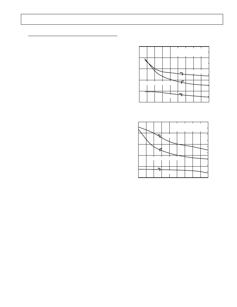
R3/R4
–
0
20
C
–
16
12
8
4
200
100
120
60
80
40
140
160
180
90
80
70
60
50
40
30
20
10
0
INPUT RF = 900MHz
OUTPUT IF = 170MHz
LO LOW SIDE INJECTION
NOISE FIGURE
GAIN
TOTAL SUPPLY CURRENT
T
–
20
100
Figure 10. Effect of R3/R4 Value on Gain and Noise Figure
R3 AND R4
–
0
20
I
–
–
20
15
10
5
200
100
120
60
80
40
140
160
180
90
80
70
60
50
40
30
20
10
0
INPUT RF = 900MHz
OUTPUT IF = 170MHz
LO LOW SIDE INJECTION
INPUT IP3
P1dB
TOTAL SUPPLY CURRENT
T
–
25
Figure 11. Effect of R3/R4 Value on Input IP3 and Gain
Compression
At low frequencies where the magnitude of the complex input
impedance is much smaller than the bias resistor values, adequate
biasing can be achieved simply by connecting a resistor from
each input to GND. The input terminals are internally biased at
1.2 V dc (nominal), so each resistor should have a resistance
value calculated as R
BIAS
= 1.2/I
BIAS
. The resistor values should
be well matched in order to maintain full LO to output isola-
tion; 1% tolerance resistors are recommended.
At higher frequencies where the input impedance of the AD8343
rises, it is beneficial to insert an inductor in series between each
bias resistor and the corresponding input pin in order to mini-
mize signal shunting (Figure 24). Practical considerations will
limit the inductive reactance to a few hundred ohms. The best
overall choice of inductor will be that value which places the
self-resonant frequency at about the upper end of the desired
input frequency range. Note that there is an RF stability con-
cern that argues in favor of erring on the side of too small an
inductor value; reference section on Input and Output Stability
Considerations. The Murata LQW1608A series of inductors
(0603 SMT package) offers values up to 56 nH before the self-
resonant frequency falls below 2.4 GHz.
相关PDF资料 |
PDF描述 |
|---|---|
| AD8343ARU | DC-to-2.5 GHz High IP3 Active Mixer |
| AD8343ARU-REEL7 | DC-to-2.5 GHz High IP3 Active Mixer |
| AD8344 | Active Receive Mixer 400 MHz to 1.2 GHz |
| AD8344-EVAL | Active Receive Mixer 400 MHz to 1.2 GHz |
| AD8344ACPZ-REEL7 | Active Receive Mixer 400 MHz to 1.2 GHz |
相关代理商/技术参数 |
参数描述 |
|---|---|
| AD8343-EVALZ | 制造商:Analog Devices 功能描述:AD8343 EVALUATION BOARD - Bulk |
| AD8344 | 制造商:AD 制造商全称:Analog Devices 功能描述:Active Receive Mixer 400 MHz to 1.2 GHz |
| AD8344ACPZ | 制造商:Analog Devices 功能描述:UP/DOWN CONV MIXER 5V 1.2GHZ 16LFCSP EP - Tape and Reel 制造商:Analog Devices 功能描述:IC SM RF MIXER 800MHZ |
| AD8344ACPZ | 制造商:Analog Devices 功能描述:IC RF MIXER 800MHZ SMD LFCSP-16 |
| AD8344ACPZ-REEL7 | 功能描述:IC MIXER 400MHZ-1.2GHZ 16-LFCSP RoHS:是 类别:RF/IF 和 RFID >> RF 混频器 系列:AD8344 产品培训模块:Lead (SnPb) Finish for COTS Obsolescence Mitigation Program 标准包装:100 系列:- RF 型:W-CDMA 频率:2.11GHz ~ 2.17GHz 混频器数目:1 增益:17dB 噪音数据:2.2dB 次要属性:- 电流 - 电源:11.7mA 电源电压:2.7 V ~ 3.3 V 包装:托盘 封装/外壳:12-VFQFN 裸露焊盘 供应商设备封装:12-QFN-EP(3x3) |
发布紧急采购,3分钟左右您将得到回复。