- 您现在的位置:买卖IC网 > PDF目录373944 > AD8343-EVAL (Analog Devices, Inc.) DC-to-2.5 GHz High IP3 Active Mixer PDF资料下载
参数资料
| 型号: | AD8343-EVAL |
| 厂商: | Analog Devices, Inc. |
| 英文描述: | DC-to-2.5 GHz High IP3 Active Mixer |
| 中文描述: | DC至2.5GHz的高IP3有源混频器 |
| 文件页数: | 3/27页 |
| 文件大小: | 394K |
| 代理商: | AD8343-EVAL |
第1页第2页当前第3页第4页第5页第6页第7页第8页第9页第10页第11页第12页第13页第14页第15页第16页第17页第18页第19页第20页第21页第22页第23页第24页第25页第26页第27页
REV. 0
AD8343
–3–
Table I. Typical AC Performance
(V
S
= 5.0 V, T
A
= 25 C; See Figure 24 and Tables III Through V.)
Input 1 dB
Compression Point
(dBm)
Input Frequency
(MHz)
Output Frequency Conversion Gain
(MHz)
SSB Noise Figure
(dB)
Input IP3
(dBm)
(dB)
RECEIVER CHARACTERISTICS
400
900
1900
2400
2400
70
170
170
170
425
5.6
3.6
7.1
6.8
5.4
10.5
11.4
14.1
15.3
16.2
20.5
19.4
16.5
14.5
16.5
3.3
3.6
2.8
2.1
2.2
TRANSMITTER CHARACTERISTICS
150
150
900
1900
7.5
0.25
17.9
16.0
18.1
13.4
1.9
0.8
Table II. Typical Isolation Performance
(V
S
= 5.0 V, T
A
= 25 C; See Figure 24 and Tables III Through V.)
Input Frequency
(MHz)
Output Frequency LO to Output
(MHz)
2
LO to Output
Leakage (dBm)
3
LO to Output
Leakage (dBm)
Input to Output
Leakage (dBm)
Leakage (dBm)
RECEIVER CHARACTERISTICS
400
900
1900
2400
2400
70
170
170
170
425
–40.1
–44.4
–65.6
–66.7
–51.1
–51.0
–35.5
–38.3
–44.4
–49.4
–44.0
< –75.0
–73.3
< –75.0
< –75.0
–62.4
–56.9
–65.7
–73.7
–52.3
TRANSMITTER CHARACTERISTICS
150
150
900
1900
–27.6
< –75 dBm
< –75 dBm
< –75 dBm
< –75 dBm
< –75 dBm
–35.3
–69.7
NOTE: Low-side LO injection used for typical performance.
ABSOLUTE MAXIMUM RATINGS
1
VPOS Quiescent Voltage . . . . . . . . . . . . . . . . . . . . . . . . 5.5 V
OUTP, OUTM Quiescent Voltage . . . . . . . . . . . . . . . . 5.5 V
INPP, INPM Voltage Differential . . . . . . . . . . . . . . . 500 mV
Internal Power Dissipation (TSSOP)
2
. . . . . . . . . . . . 320 mW
θ
JA
(TSSOP) . . . . . . . . . . . . . . . . . . . . . . . . . . . . . . 125
°
C/W
Maximum Junction Temperature . . . . . . . . . . . . . . . . . 125
°
C
Operating Temperature Range . . . . . . . . . . . –40
°
C to +85
°
C
Storage Temperature Range . . . . . . . . . . . . –65
°
C to +150
°
C
Lead Temperature Range (Soldering 60 sec) . . . . . . . . . 300
°
C
NOTES
1
Stresses above those listed under Absolute Maximum Ratings may cause perma-
nent damage to the device. This is a stress rating only; functional operation of the
device at these or any other conditions above those indicated in the operational
section of this specification is not implied. Exposure to absolute maximum rating
conditions for extended periods may effect device reliability.
2
A portion of the device power is dissipated by the external bias resistors R3 and R4.
ORDERING GUIDE
Model
Temperature Range
Package Description
Package Option
AD8343ARU
AD8343ARU-REEL
AD8343ARU-REEL7
AD8343-EVAL
RU-14
13" Tape and Reel
7" Tape and Reel
Evaluation Board
–40
°
C to +85
°
C
14-Lead Plastic TSSOP
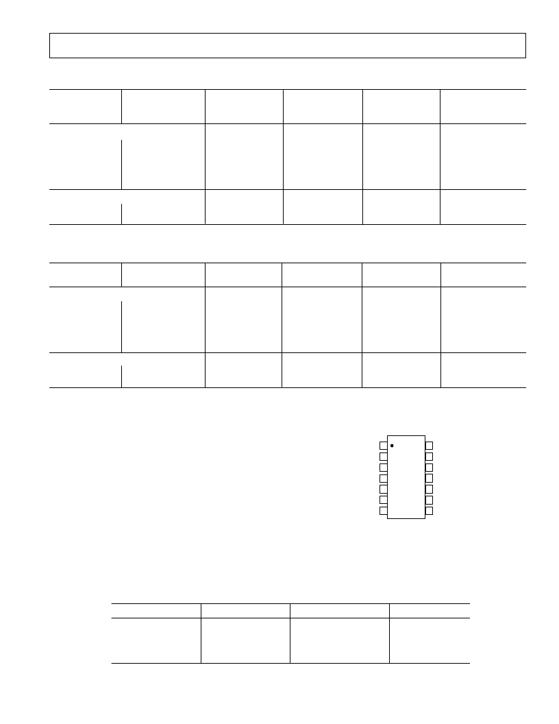
PIN CONFIGURATION
TOP VIEW
(Not to Scale)
14
13
12
11
10
9
8
1
2
3
4
5
6
7
COMM
AD8343
INPP
INPM
DCPL
VPOS
PWDN
COMM
COMM
OUTP
OUTM
COMM
LOIP
LOIM
COMM
相关PDF资料 |
PDF描述 |
|---|---|
| AD8343ARU | DC-to-2.5 GHz High IP3 Active Mixer |
| AD8343ARU-REEL7 | DC-to-2.5 GHz High IP3 Active Mixer |
| AD8344 | Active Receive Mixer 400 MHz to 1.2 GHz |
| AD8344-EVAL | Active Receive Mixer 400 MHz to 1.2 GHz |
| AD8344ACPZ-REEL7 | Active Receive Mixer 400 MHz to 1.2 GHz |
相关代理商/技术参数 |
参数描述 |
|---|---|
| AD8343-EVALZ | 制造商:Analog Devices 功能描述:AD8343 EVALUATION BOARD - Bulk |
| AD8344 | 制造商:AD 制造商全称:Analog Devices 功能描述:Active Receive Mixer 400 MHz to 1.2 GHz |
| AD8344ACPZ | 制造商:Analog Devices 功能描述:UP/DOWN CONV MIXER 5V 1.2GHZ 16LFCSP EP - Tape and Reel 制造商:Analog Devices 功能描述:IC SM RF MIXER 800MHZ |
| AD8344ACPZ | 制造商:Analog Devices 功能描述:IC RF MIXER 800MHZ SMD LFCSP-16 |
| AD8344ACPZ-REEL7 | 功能描述:IC MIXER 400MHZ-1.2GHZ 16-LFCSP RoHS:是 类别:RF/IF 和 RFID >> RF 混频器 系列:AD8344 产品培训模块:Lead (SnPb) Finish for COTS Obsolescence Mitigation Program 标准包装:100 系列:- RF 型:W-CDMA 频率:2.11GHz ~ 2.17GHz 混频器数目:1 增益:17dB 噪音数据:2.2dB 次要属性:- 电流 - 电源:11.7mA 电源电压:2.7 V ~ 3.3 V 包装:托盘 封装/外壳:12-VFQFN 裸露焊盘 供应商设备封装:12-QFN-EP(3x3) |
发布紧急采购,3分钟左右您将得到回复。