- 您现在的位置:买卖IC网 > PDF目录97841 > AD8343ARUZ-REEL7 (ANALOG DEVICES INC) 0 MHz - 2500 MHz RF/MICROWAVE DOUBLE BALANCED MIXER PDF资料下载
参数资料
| 型号: | AD8343ARUZ-REEL7 |
| 厂商: | ANALOG DEVICES INC |
| 元件分类: | 混频器 |
| 英文描述: | 0 MHz - 2500 MHz RF/MICROWAVE DOUBLE BALANCED MIXER |
| 封装: | LEAD FREE, PLASTIC, TSSOP-14 |
| 文件页数: | 19/32页 |
| 文件大小: | 2171K |
| 代理商: | AD8343ARUZ-REEL7 |
第1页第2页第3页第4页第5页第6页第7页第8页第9页第10页第11页第12页第13页第14页第15页第16页第17页第18页当前第19页第20页第21页第22页第23页第24页第25页第26页第27页第28页第29页第30页第31页第32页
AD8343
Rev. B | Page 26 of 32
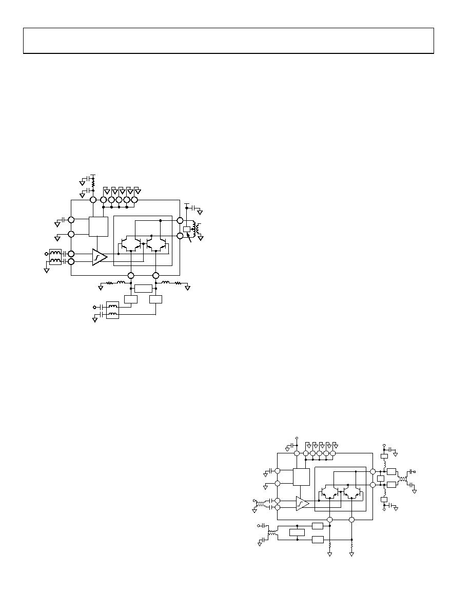
APPLICATIONS
DOWNCONVERTING MIXER
A typical downconversion application is shown in Figure 69
with the AD8343 connected as a receive mixer. The input
single-ended-to-differential conversion is obtained through
the use of a 1:1 transmission line balun. The input matching
network is positioned between the balun and the input pins,
while the output is taken directly from a 4:1 impedance ratio
(2:1 turns ratio) transformer. The local oscillator signal at a level
of –12 dBm to –3 dBm is brought in through a second 1:1 balun.
BIAS
AD8343
VPOS
DCPL
PWDN
LOIP
LOIM
INPP
INPM
OU
TP
OU
TM
COMM
4
6
2
3
12
13
14
11
8
7
1
5
01034
-069
LO IN
–10dBm
10
9
VPOS
4.71
IFOUT
FB
4:1
FERRITE BEAD
VPOS
L1B
L1A
R1A
68
R1B
68
RFIN
Z1
Z2A
1:1
Z2B
0.1F
1:1
Figure 69. Typical Downconversion Application
R1A and R1B set the core bias current of 18.5 mA per side. L1A
and L1B provide the RF choking required to avoid shunting the
signal. Z1, Z2A, and Z2B comprise a typical input matching
network that is designed to match the AD8343s differential
input impedance to the differential output impedance of the
balun.
The IF output is taken through a 4:1 (impedance ratio) trans-
former that reflects a 200 Ω differential load to the collectors.
This output coupling arrangement is reasonably broadband,
although in some cases the user might want to consider adding
a resonator tank circuit between the collectors to provide a
measure of IF selectivity. The ferrite bead (FB), in series with
the output transformer’s center tap, addresses the common-
mode stability concern.
In this circuit, the PWDN pin is shown connected to GND,
enabling the mixer. In order to enter power-down mode and
conserve power, the PWDN pin must be taken within 500 mV
of VPOS. The DCPL pin is bypassed to GND with about 0.1 μF.
Failure to do so results in a higher noise level at the output of
the device.
UPCONVERTING MIXER
A typical upconversion application is shown in Figure 70. Both
the input and output single-ended-to-differential conversions
are obtained through the use of 1:1 transmission line baluns.
The differential input and output matching networks are
designed between the balun and the I/O pins of the AD8343.
The local oscillator signal at a level of –12 dBm to –3 dBm is
brought in through a third 1:1 balun.
R1A and R1B set the core bias current of 18 mA per side. Z1,
Z2A, and Z2B comprise a typical input matching network
designed to match the AD8343s differential input impedance
to the differential output impedance of the balun. It is assumed
for this example that the input frequency is low and that the
magnitude of the device’s input impedance is therefore much
smaller than the bias resistor values, allowing the input bias
inductors to be eliminated with very little penalty in gain or
noise performance.
In this example, the output signal is taken via a differential
matching network comprising Z3 and Z4A/Z4B, then
through the 1:1 balun and dc blocking capacitors to the
single-ended output.
The output frequency is assumed to be high enough that
conjugate matching to the output of the AD8343 is desirable,
so the goal of the matching network is to provide a conjugate
match between the device’s output and the differential input of
the output balun.
This circuit uses shunt feed to provide collector bias for the
transistors because the output balun in this circuit has no
convenient center-tap. The ferrite beads, in series with the
output’s bias inductors, provide some small degree of damping
to ease the common-mode stability problem. Unfortunately, this
type of output balun can present a common-mode load that
enters the region of output instability, so most of the burden of
avoiding overt instability falls on the input circuit, presenting an
inductive common-mode termination over as broad a band of
frequencies as possible.
The PWDN pin is shown as tied to GND, enabling the mixer.
The DCPL pin must be bypassed to GND with about 0.1 μF to
bypass noise from the internal bias circuit.
BIAS
AD8343
VPOS
DCPL
PWDN
LOIP
LOIM
INPP
INPM
OU
TP
OU
TM
COMM
LO
DRIVER
4
6
2
3
12
13
14
11
8
7
1
5
010
34-
070
10
9
VPOS
RFIN
Z1
Z2A
Z2B
LO IN
RFOUT
VPOS
FB
Z3
Z4A
FB
Z4B
R1A
R1B
0.1F
Figure 70. Typical Upconversion Application
相关PDF资料 |
PDF描述 |
|---|---|
| AD8343ARUZ-REEL | 0 MHz - 2500 MHz RF/MICROWAVE DOUBLE BALANCED MIXER |
| AD8345AREZ1 | 140 MHz - 1000 MHz RF/MICROWAVE QUADRAPHASE MODULATOR |
| AD8345AREZ-RL7 | 140 MHz - 1000 MHz RF/MICROWAVE QUADRAPHASE MODULATOR |
| AD8345AREZ-REEL7 | 140 MHz - 1000 MHz RF/MICROWAVE QUADRAPHASE MODULATOR |
| AD8346ARUZ-REEL | 800 MHz - 2500 MHz RF/MICROWAVE I/Q MODULATOR |
相关代理商/技术参数 |
参数描述 |
|---|---|
| AD8343-EVAL | 制造商:Analog Devices 功能描述:AD8343 EVALUATION BOARD - Bulk |
| AD8343-EVALZ | 制造商:Analog Devices 功能描述:AD8343 EVALUATION BOARD - Bulk |
| AD8344 | 制造商:AD 制造商全称:Analog Devices 功能描述:Active Receive Mixer 400 MHz to 1.2 GHz |
| AD8344ACPZ | 制造商:Analog Devices 功能描述:UP/DOWN CONV MIXER 5V 1.2GHZ 16LFCSP EP - Tape and Reel 制造商:Analog Devices 功能描述:IC SM RF MIXER 800MHZ |
| AD8344ACPZ | 制造商:Analog Devices 功能描述:IC RF MIXER 800MHZ SMD LFCSP-16 |
发布紧急采购,3分钟左右您将得到回复。