参数资料
| 型号: | AD8370ARE-REEL7 |
| 厂商: | Analog Devices Inc |
| 文件页数: | 5/28页 |
| 文件大小: | 0K |
| 描述: | IC AMP VGA DIFF LN 16TSSOP |
| 标准包装: | 1,000 |
| 放大器类型: | 可变增益 |
| 电路数: | 1 |
| 输出类型: | 差分 |
| 转换速率: | 5750 V/ns |
| -3db带宽: | 750MHz |
| 电流 - 输入偏压: | 400pA |
| 电流 - 电源: | 79mA |
| 电压 - 电源,单路/双路(±): | 3 V ~ 5.5 V |
| 工作温度: | -40°C ~ 85°C |
| 安装类型: | 表面贴装 |
| 封装/外壳: | 16-TSSOP(0.173",4.40mm)裸露焊盘 |
| 供应商设备封装: | 16-TSSOP-EP |
| 包装: | 带卷 (TR) |
第1页第2页第3页第4页当前第5页第6页第7页第8页第9页第10页第11页第12页第13页第14页第15页第16页第17页第18页第19页第20页第21页第22页第23页第24页第25页第26页第27页第28页

Data Sheet
AD8370
Rev. B | Page 13 of 28
THEORY OF OPERATION
The AD8370 is a low cost, digitally controlled, fine adjustment
variable gain amplifier (VGA) that provides both high IP3 and
low noise figure. The AD8370 is fabricated on an ADI proprietary
high performance 25 GHz silicon bipolar process. The –3 dB
bandwidth is approximately 750 MHz throughout the variable
gain range. The typical quiescent current of the AD8370 is
78 mA. A power-down feature reduces the current to less than
4 mA. The input impedance is approximately 200 differential,
and the output impedance is approximately 100 differential
to be compatible with saw filters and matching networks used
in intermediate frequency (IF) radio applications. Because there
is no feedback between the input and output and stages within
the amplifier, the input amplifier is isolated from variations in
output loading and from subsequent impedance changes, and
excellent input to output isolation is realized. Excellent distortion
performance and wide bandwidth make the AD8370 a suitable
gain control device for modern differential receiver designs. The
AD8370 differential input and output configuration is ideally
suited to fully differential signal chain circuit designs, although
it can be adapted to single-ended system applications, if required.
BLOCK ARCHITECTURE
The three basic building blocks of the AD8370 are a high/low
gain selectable input preamplifier, a digitally controlled
transconductance (gm) block, and a fixed gain output stage.
INHI
INLO
OPHI
OPLO
VCCO
OCOM
ICOM
VOCM
PWUP
VCCO
OCOM
VCCI
ICOM
BIAS CELL
SHIFT REGISTER
AND LATCHES
PRE
AMP
TRANSCONDUCTANCE
OUTPUT
AMP
11
6
1
16
4
14
13
12
5
9
8
3
2
10
7
15
DATA CLCK LTCH
AD8370
03692-035
Figure 37. Functional Block Diagram
PREAMPLIFIER
There are two selectable input preamplifiers. Selection is made
by the most significant bit (MSB) of the serial gain control data-
word. In the high gain mode, the overall device gain is 7.1 V/V
(17 dB) above the low gain setting. The two preamplifiers give
the AD8370 the ability to accommodate a wide range of input
amplitudes. The overlap between the two gain ranges allows the
user some flexibility based on noise and distortion demands.
See the Choosing Between Gain Ranges section for more
information.
The input impedance is approximately 200 differential,
regardless of which preamplifier is selected. Note that the input
impedance is formed by using active circuit elements and is not
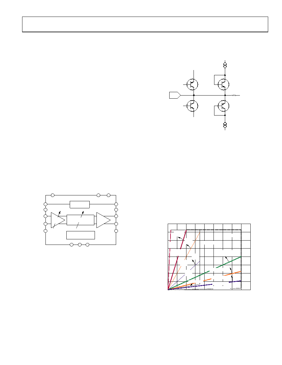
set by passive components. See Figure 38 for a simplified
schematic of the input interface.
1mA
VCC/2
2k
INHI/INLO
03692-
036
Figure 38. INHI/INLO Simplified Schematic
TRANSCONDUCTANCE STAGE
The digitally controlled gm section has 42 dB of controllable
gain and makes gain adjustments within each gain range. The
step size resolution ranges from a fine ~ 0.07 dB up to a coarse
6 dB per bit, depending on the gain code. As shown in Figure 39,
of the 42 dB total range, 28 dB has resolution of better than
2 dB, and 22 dB has resolution of better than 1 dB.
Figure 39 shows typical input levels that can be applied to this
amplifier at different gain settings. The maximum input was
determined by finding the 1 dB compression or expansion point
of the VOUT/VSOURCE gain. Note that this is not VOUT/VIN. In this
way, the change in the input impedance of the device is also
taken into account.
0
0.4
0.8
1.2
1.6
2.0
V
OUT
[V
peak]
(V)
2.4
2.8
3.2
0
0.2
0.4
0.6
0.8
1.0
1.2
1.4
1.6
1.8
VSOURCE [V peak] (V)
03692-037
HIGH GAIN
0.1dB GAIN
–5dB GAIN
–8dB GAIN
12dB
GAIN
6dB
GAIN
<2dB
RES
<2dB
RES
<1dB
RES
<1dB
RES
<0.5dB
RESOLUTION
<0.5dB
RES
–11dB GAIN
17dB
GAIN
34dB
GAIN
–25dB GAIN
LOW GAIN
Figure 39. Gain Resolution and Nominal Input and
Output Range over the Gain Range
相关PDF资料 |
PDF描述 |
|---|---|
| AD8372ACPZ-R7 | IC AMP VGA DIFF DUAL LN 32LFCSP |
| AD8375ACPZ-R7 | IC AMP VGA DIFF ULDIST 24LFCSP |
| AD8376ACPZ-R7 | IC AMP VGA DIFF DUAL 32LFCSP |
| AD8390AACPZ-R2 | IC AMP DIFF LP LDIST 16LFCSP |
| AD8390ACPZ-REEL7 | IC AMP DIFF LP LDIST 16LFCSP |
相关代理商/技术参数 |
参数描述 |
|---|---|
| AD8370AREZ | 功能描述:IC AMP VGA DIFF LN 16TSSOP RoHS:是 类别:集成电路 (IC) >> Linear - Amplifiers - Instrumentation 系列:- 标准包装:2,500 系列:- 放大器类型:通用 电路数:4 输出类型:- 转换速率:0.6 V/µs 增益带宽积:1MHz -3db带宽:- 电流 - 输入偏压:45nA 电压 - 输入偏移:2000µV 电流 - 电源:1.4mA 电流 - 输出 / 通道:40mA 电压 - 电源,单路/双路(±):3 V ~ 32 V,±1.5 V ~ 16 V 工作温度:0°C ~ 70°C 安装类型:表面贴装 封装/外壳:14-TSSOP(0.173",4.40mm 宽) 供应商设备封装:14-TSSOP 包装:带卷 (TR) 其它名称:LM324ADTBR2G-NDLM324ADTBR2GOSTR |
| AD8370AREZ | 制造商:Analog Devices 功能描述:IC VARIABLE GAIN AMP 750MHZ TSSOP-16 制造商:Analog Devices 功能描述:IC, VARIABLE GAIN AMP, 750MHZ, TSSOP-16 |
| AD8370AREZ1 | 制造商:AD 制造商全称:Analog Devices 功能描述:LF to 750 MHz, Digitally Controlled VGA |
| AD8370AREZ-RL7 | 功能描述:IC AMP VGA DIFF LN 16TSSOP RoHS:是 类别:集成电路 (IC) >> Linear - Amplifiers - Instrumentation 系列:- 标准包装:150 系列:- 放大器类型:音频 电路数:2 输出类型:- 转换速率:5 V/µs 增益带宽积:12MHz -3db带宽:- 电流 - 输入偏压:100nA 电压 - 输入偏移:500µV 电流 - 电源:6mA 电流 - 输出 / 通道:50mA 电压 - 电源,单路/双路(±):4 V ~ 32 V,±2 V ~ 16 V 工作温度:-40°C ~ 85°C 安装类型:表面贴装 封装/外壳:8-TSSOP(0.173",4.40mm 宽) 供应商设备封装:8-TSSOP 包装:管件 |
| AD8370-EVAL | 制造商:Analog Devices 功能描述:AD8370 EVAL BOARD - Bulk |
发布紧急采购,3分钟左右您将得到回复。