参数资料
| 型号: | AD842KNZ |
| 厂商: | Analog Devices Inc |
| 文件页数: | 16/16页 |
| 文件大小: | 0K |
| 描述: | IC OPAMP GP 80MHZ 100MA 14DIP |
| 标准包装: | 25 |
| 放大器类型: | 通用 |
| 电路数: | 1 |
| 转换速率: | 375 V/µs |
| 增益带宽积: | 80MHz |
| 电流 - 输入偏压: | 3.5µA |
| 电压 - 输入偏移: | 300µV |
| 电流 - 电源: | 13mA |
| 电流 - 输出 / 通道: | 100mA |
| 电压 - 电源,单路/双路(±): | ±5 V ~ 18 V |
| 工作温度: | 0°C ~ 75°C |
| 安装类型: | 通孔 |
| 封装/外壳: | 14-DIP(0.300",7.62mm) |
| 供应商设备封装: | 14-PDIP |
| 包装: | 管件 |
Data Sheet
AD842
THEORY OF OPERATION
OFFSET NULLING
The input offset voltage of the AD842 is very low for a high
speed op amp, but if additional nulling is required, the circuit
shown in Figure 28 can be used.
SETTLING TIME
Figure 29 and Figure 31 show the settling performance of the
AD842 in the test circuit shown in Figure 30.
Settling time is the interval of time from the application of an
ideal step function input until the closed-loop amplifier output
enters and remains within a specified error band.
This definition encompasses the major components that
comprise settling time. They include the following:
Propagation delay through the amplifier.
Slewing time to approach the final output value.
Time of recovery from the overload associated with
slewing.
Linear settling to within the specified error band.
Expressed in these terms, the measurement of settling time
must be accurate to assure the user that the amplifier is worth
consideration for the application.
Figure 28. Offset Nulling (PDIP)
Figure 29. 0.01% Settling Time
Figure 30 shows how measurement of the AD842 0.01% settling
in 100 ns is accomplished by amplifying the error signal from a
false summing junction with a very high speed proprietary
hybrid error amplifier specially designed to enable testing of
small settling errors. Under test, the device drives a 300 Ω load.
The input to the error amp is clamped to avoid possible
problems associated with the overdrive recovery of the
oscilloscope input amplifier. The error amp gains the error from
the false summing junction by 15, and it contains a gain vernier
to fine trim the gain.
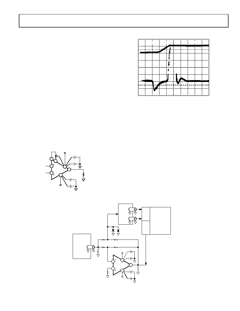
Figure 31 shows the long-term stability of the settling
characteristics of the AD842 output after a 10 V step. There is
no evidence of settling tails after the initial transient recovery
time. The use of a junction isolated process, together with
careful layout, avoids these problems by minimizing the effects
of transistor isolation capacitance discharge and thermally
induced shifts in circuit operating points. These problems do
not occur even under high output current conditions.
Figure 30. Settling Time Test Circuit (PDIP)
+VS
–VS
VOUT
RL
2.2F
0.1F
2.2F
0.1F
10k
VIN
AD842
11
3
13
6
10
4
5
09477-
028
09477-
029
100%
90%
0%
10%
10mV
10V
20ns
OUTPUT:
10V/DIV
OUTPUT
ERROR:
0.02%/DIV
2.2F
0.1F
2.2F
0.1F
499
–15V
DDD5109
FLAT-TOP
PULSE
GENERATOR
50
499
1k
499
1k
+15V
HP6263
ERROR
AMP
(×15)
TEK
7603
OSCILLOSCOPE
TEK
7A13
TEK
7A16
FET PROBE
TEK P6201
AD842
11
6
10
4
5
09477-
030
Rev. F | Page 9 of 16
相关PDF资料 |
PDF描述 |
|---|---|
| DF7-6P-3.96DS | CONN HEADER 6POS 3.96MM RT ANG T |
| TSM-108-01-TM-DV-P | CONN HEADER 16POS .100" DBL SMD |
| OP467GS-REEL | IC OPAMP GP 28MHZ QUAD 16SOIC |
| DF7-5P-3.96DS | CONN HEADER 5POS 3.96MM RT ANG T |
| RC0201JR-0768KL | RES 68K OHM 1/20W 5% 0201 SMD |
相关代理商/技术参数 |
参数描述 |
|---|---|
| AD842KQ | 功能描述:IC OPAMP GP 80MHZ 100MA 14CDIP RoHS:否 类别:集成电路 (IC) >> Linear - Amplifiers - Instrumentation 系列:- 标准包装:2,500 系列:Excalibur™ 放大器类型:J-FET 电路数:1 输出类型:- 转换速率:45 V/µs 增益带宽积:10MHz -3db带宽:- 电流 - 输入偏压:20pA 电压 - 输入偏移:490µV 电流 - 电源:1.7mA 电流 - 输出 / 通道:48mA 电压 - 电源,单路/双路(±):4.5 V ~ 38 V,±2.25 V ~ 19 V 工作温度:-40°C ~ 85°C 安装类型:表面贴装 封装/外壳:8-SOIC(0.154",3.90mm 宽) 供应商设备封装:8-SOIC 包装:带卷 (TR) |
| AD842SCHIPS | 制造商:AD 制造商全称:Analog Devices 功能描述:Wideband, High Output Current, Fast Settling Op Amp |
| AD842SE | 制造商:未知厂家 制造商全称:未知厂家 功能描述:Voltage-Feedback Operational Amplifier |
| ad842se/883b | 制造商:Analog Devices 功能描述:OP AMP SGL GP 18V 20PIN LCC - Rail/Tube 制造商:Rochester Electronics LLC 功能描述:HIGH OUTPUT CURRENT AMP - Bulk |
| AD842SH | 制造商:Rochester Electronics LLC 功能描述:HIGH OUTPUT CURRENT AMP - Bulk 制造商:Analog Devices 功能描述: |
发布紧急采购,3分钟左右您将得到回复。