参数资料
| 型号: | AD842KNZ |
| 厂商: | Analog Devices Inc |
| 文件页数: | 2/16页 |
| 文件大小: | 0K |
| 描述: | IC OPAMP GP 80MHZ 100MA 14DIP |
| 标准包装: | 25 |
| 放大器类型: | 通用 |
| 电路数: | 1 |
| 转换速率: | 375 V/µs |
| 增益带宽积: | 80MHz |
| 电流 - 输入偏压: | 3.5µA |
| 电压 - 输入偏移: | 300µV |
| 电流 - 电源: | 13mA |
| 电流 - 输出 / 通道: | 100mA |
| 电压 - 电源,单路/双路(±): | ±5 V ~ 18 V |
| 工作温度: | 0°C ~ 75°C |
| 安装类型: | 通孔 |
| 封装/外壳: | 14-DIP(0.300",7.62mm) |
| 供应商设备封装: | 14-PDIP |
| 包装: | 管件 |
AD842
Data Sheet
GROUNDING AND BYPASSING
In designing practical circuits with the AD842, the user must
take some special precautions whenever high frequencies are
involved.
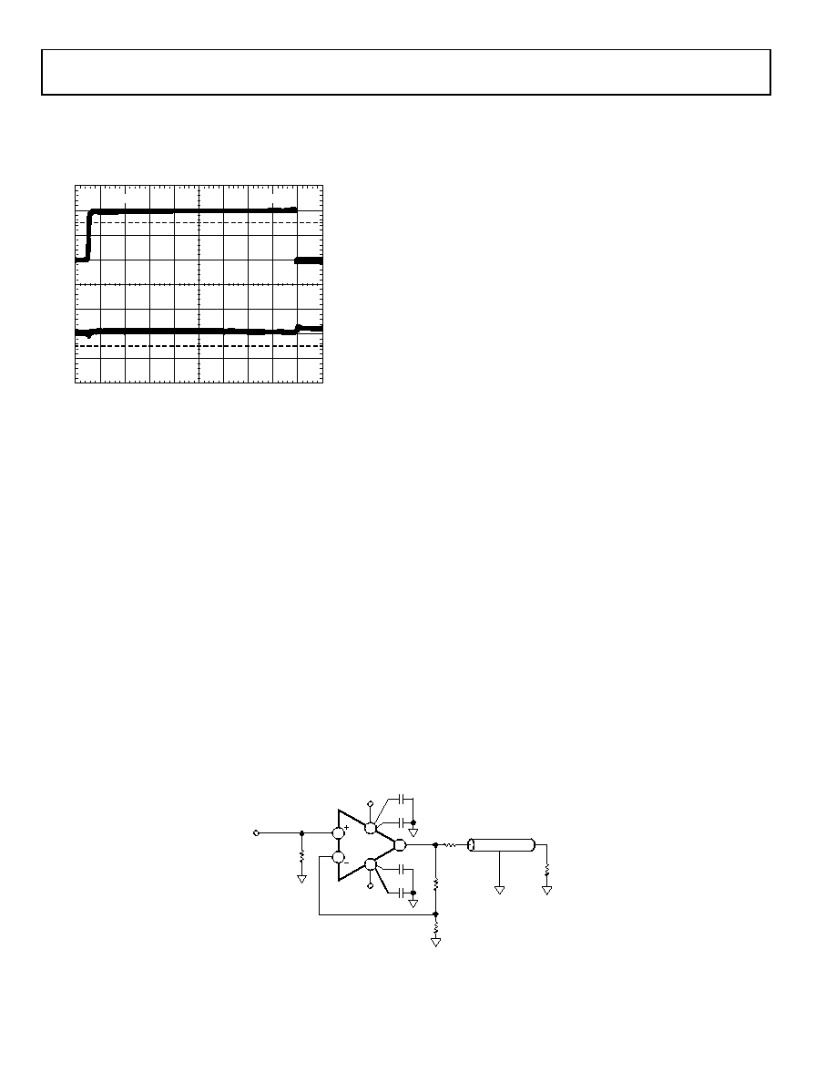
Figure 31. AD842 Settling Demonstrating No Settling Tails
Circuits must be built with short interconnect leads. Use large
ground planes whenever possible to provide a low resistance,
low inductance circuit path; this also minimizes the effects of
high frequency coupling. Avoid sockets because the increased
interlead capacitance can degrade bandwidth.
Use feedback resistors of low enough value to ensure that the
time constant formed with the circuit capacitances does not
limit the amplifier performance. Resistor values of less than
5 kΩ are recommended. If a larger resistor must be used, a
small (<10 pF) feedback capacitor connected in parallel with
the feedback resistor, RF, can be used to compensate for these
stray capacitances and to optimize the dynamic performance of
the amplifier in the particular application.
Bypass power supply leads to ground as close as possible to the
amplifier pins. A 2.2 μF capacitor in parallel with a 0.1 μF
ceramic disk capacitor is recommended.
CAPACITIVE LOAD DRIVING ABILITY
Like all wideband amplifiers, the AD842 is sensitive to
capacitive loading. The AD842 is designed to drive capacitive
loads of up to 20 pF without degradation of its rated
performance. Capacitive loads of greater than 20 pF decrease
the dynamic performance of the device, although instability
does not occur unless the load exceeds 100 pF.
USING A HEAT SINK
The AD842 draws less quiescent power than most precision
high speed amplifiers and is specified for operation without a
heat sink. However, when driving low impedance loads, the
current to the load can be 10 times the quiescent current. This
creates a noticeable temperature rise. Use of a small heat sink
improves performance.
TERMINATED LINE DRIVER
The AD842 is optimized for high speed line driver applications.
Figure 32 shows the AD842 driving a doubly terminated cable
in a gain-of-2 follower configuration. The AD842 maintains a
typical slew rate of 375 V/μs, which means it can drive a ±10 V,
6.0 MHz signal, or a ±3 V, 19.9 MHz signal.
The termination resistor, RT, minimizes reflections from the far
end of the cable when equal to the characteristic impedance of
the cable. A back-termination resistor (RBT, also equal to the
characteristic impedance of the cable) can be placed between
the AD842 output and the cable to damp any stray signals
caused by a mismatch between RT and the characteristic
impedance of the cable. This configuration results in a cleaner
signal. With this circuit, the voltage on the line equals VIN
because one half of VOUT is dropped across RBT.
The AD842 has a 100 mA minimum output current and,
therefore, can drive ±5 V into a 50 Ω cable.
Choose the feedback resistors, R1 and R2, carefully. Large value
resistors are desirable to limit the amount of current drawn
from the amplifier output. Large resistors can cause amplifier
instability because the parallel resistance of R1||R2 combines
with the input capacitance (typically 2 pF to 5 pF) to create an
additional pole. The voltage noise of the AD842 is equivalent to
a 5 kΩ resistor; these large resistors can significantly increase
the system noise. Resistor values of 1 kΩ or 2 kΩ are
recommended.
If termination is not used, cables appear as capacitive loads and
can be decoupled from the AD842 by a resistor in series with
the output.
Figure 32. Line Driver Configuration (PDIP)
09477-
031
100%
90%
0%
10%
5mV
2s
OUTPUT:
5V/DIV
OUTPUT
ERROR:
0.01%/DIV
2.2F
0.1F
50 OR 75
CABLE
RT = RBT = CABLE
CHARACTERISTIC IMPEDANCE
2.2F
0.1F
R1
R2
–VS
+VS
VIN
AD842
11
6
10
4
5
4
RT
RBT
TERMINATION
RESISTOR FOR
INPUT SIGNAL
09477-
032
Rev. F | Page 10 of 16
相关PDF资料 |
PDF描述 |
|---|---|
| DF7-6P-3.96DS | CONN HEADER 6POS 3.96MM RT ANG T |
| TSM-108-01-TM-DV-P | CONN HEADER 16POS .100" DBL SMD |
| OP467GS-REEL | IC OPAMP GP 28MHZ QUAD 16SOIC |
| DF7-5P-3.96DS | CONN HEADER 5POS 3.96MM RT ANG T |
| RC0201JR-0768KL | RES 68K OHM 1/20W 5% 0201 SMD |
相关代理商/技术参数 |
参数描述 |
|---|---|
| AD842KQ | 功能描述:IC OPAMP GP 80MHZ 100MA 14CDIP RoHS:否 类别:集成电路 (IC) >> Linear - Amplifiers - Instrumentation 系列:- 标准包装:2,500 系列:Excalibur™ 放大器类型:J-FET 电路数:1 输出类型:- 转换速率:45 V/µs 增益带宽积:10MHz -3db带宽:- 电流 - 输入偏压:20pA 电压 - 输入偏移:490µV 电流 - 电源:1.7mA 电流 - 输出 / 通道:48mA 电压 - 电源,单路/双路(±):4.5 V ~ 38 V,±2.25 V ~ 19 V 工作温度:-40°C ~ 85°C 安装类型:表面贴装 封装/外壳:8-SOIC(0.154",3.90mm 宽) 供应商设备封装:8-SOIC 包装:带卷 (TR) |
| AD842SCHIPS | 制造商:AD 制造商全称:Analog Devices 功能描述:Wideband, High Output Current, Fast Settling Op Amp |
| AD842SE | 制造商:未知厂家 制造商全称:未知厂家 功能描述:Voltage-Feedback Operational Amplifier |
| ad842se/883b | 制造商:Analog Devices 功能描述:OP AMP SGL GP 18V 20PIN LCC - Rail/Tube 制造商:Rochester Electronics LLC 功能描述:HIGH OUTPUT CURRENT AMP - Bulk |
| AD842SH | 制造商:Rochester Electronics LLC 功能描述:HIGH OUTPUT CURRENT AMP - Bulk 制造商:Analog Devices 功能描述: |
发布紧急采购,3分钟左右您将得到回复。