- 您现在的位置:买卖IC网 > PDF目录3529 > AD8510BR-REEL (Analog Devices Inc)IC OPAMP JFET 8MHZ PREC LN 8SOIC PDF资料下载
参数资料
| 型号: | AD8510BR-REEL |
| 厂商: | Analog Devices Inc |
| 文件页数: | 6/20页 |
| 文件大小: | 0K |
| 描述: | IC OPAMP JFET 8MHZ PREC LN 8SOIC |
| 设计资源: | Versatile High Precision Programmable Current Sources Using DACs, Op Amps, and MOSFET Transistors (CN0151) |
| 标准包装: | 2,500 |
| 放大器类型: | J-FET |
| 电路数: | 1 |
| 转换速率: | 20 V/µs |
| 增益带宽积: | 8MHz |
| 电流 - 输入偏压: | 25pA |
| 电压 - 输入偏移: | 80µV |
| 电流 - 电源: | 2.2mA |
| 电流 - 输出 / 通道: | 70mA |
| 电压 - 电源,单路/双路(±): | ±4.5 V ~ 18 V |
| 工作温度: | -40°C ~ 125°C |
| 安装类型: | 表面贴装 |
| 封装/外壳: | 8-SOIC(0.154",3.90mm 宽) |
| 供应商设备封装: | 8-SO |
| 包装: | 带卷 (TR) |
AD8510/AD8512/AD8513
Rev. I | Page 14 of 20
SETTLING TIME
Settling time is the time it takes the output of the amplifier to
reach and remain within a percentage of its final value after a
pulse is applied at the input. The AD8510/AD8512/AD8513
settle to within 0.01% in less than 900 ns with a step of 0 V to
10 V in unity gain. This makes each of these parts an excellent
choice as a buffer at the output of DACs whose settling time is
typically less than 1 μs.
In addition to the fast settling time and fast slew rate, low offset
voltage drift and input offset current maintain the full accuracy
of 12-bit converters over the entire operating temperature range.
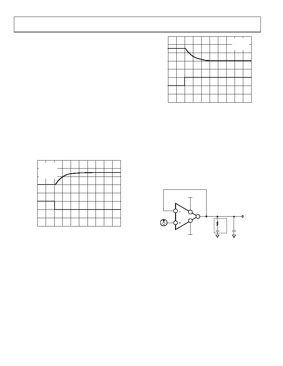
OVERLOAD RECOVERY TIME
Overload recovery, also known as overdrive recovery, is the
time it takes the output of an amplifier to recover to its linear
region from a saturated condition. This recovery time is par-
ticularly important in applications where the amplifier must
amplify small signals in the presence of large transient voltages.
Figure 43 shows the positive overload recovery of the AD8510/
AD8512/AD8513. The output recovers in approximately 200 ns
from a saturated condition.
0V
–15V
200mV
0V
OU
TP
U
T
IN
P
U
T
VO
LT
AG
E
TIME (2s/DIV)
VSY = ±15V
VIN = 200mV
AV = –100
RL = 10k
02
72
9-
05
3
Figure 43. Positive Overload Recovery
The negative overdrive recovery time shown in Figure 44 is less
than 200 ns.
In addition to the fast recovery time, the AD8510/AD8512/
AD8513 show excellent symmetry of the positive and negative
recovery times. This is an important feature for transient signal
rectification because the output signal is kept equally undistorted
throughout any given period.
TIME (2s/DIV)
VOL
TA
G
E
–200mV
0V
+15V
02
72
9-
0
54
IN
P
U
T
OU
T
P
U
T
VSY = ±15V
AV = –100
RL = 10k
Figure 44. Negative Overload Recovery
CAPACITIVE LOAD DRIVE
The AD8510/AD8512/AD8513 are unconditionally stable at all
gains in inverting and noninverting configurations. Each device
is capable of driving a capacitive load of up to 1000 pF without
oscillation in unity gain using the worst-case configuration.
However, as with most amplifiers, driving larger capacitive
loads in a unity gain configuration may cause excessive
overshoot and ringing, or even oscillation. A simple snubber
network significantly reduces the amount of overshoot and
ringing. The advantage of this configuration is that the output
swing of the amplifier is not reduced, because RS is outside the
feedback loop.
7
4
6
AD8510
200mV
RS
CS
CL
VOUT
V+
V–
02
72
9-
0
55
2
3
Figure 45. Snubber Network Configuration
相关PDF资料 |
PDF描述 |
|---|---|
| C1Q 500 | FUSE 500MA 125V 1206 FAST C1Q |
| AD8042ARZ-REEL7 | IC OPAMP VF R-R DUAL LP 8SOIC |
| AD8032ARM-REEL7 | IC OPAMP VF R-R DUAL LP 8MSOP |
| LT1999HMS8-10#PBF | IC OP AMP CURRENT SENSE 8MSOP |
| C1Q 5 | FUSE 5A 125V 1206 FAST C1Q |
相关代理商/技术参数 |
参数描述 |
|---|---|
| AD8510BR-REEL7 | 制造商:Analog Devices 功能描述:OP Amp Single GP 制造商:Analog Devices 功能描述:OP Amp Single GP ±15V 8-Pin SOIC N T/R |
| AD8510BRZ | 功能描述:IC OPAMP JFET 8MHZ PREC LN 8SOIC RoHS:是 类别:集成电路 (IC) >> Linear - Amplifiers - Instrumentation 系列:- 标准包装:2,500 系列:- 放大器类型:通用 电路数:4 输出类型:- 转换速率:0.6 V/µs 增益带宽积:1MHz -3db带宽:- 电流 - 输入偏压:45nA 电压 - 输入偏移:2000µV 电流 - 电源:1.4mA 电流 - 输出 / 通道:40mA 电压 - 电源,单路/双路(±):3 V ~ 32 V,±1.5 V ~ 16 V 工作温度:0°C ~ 70°C 安装类型:表面贴装 封装/外壳:14-TSSOP(0.173",4.40mm 宽) 供应商设备封装:14-TSSOP 包装:带卷 (TR) 其它名称:LM324ADTBR2G-NDLM324ADTBR2GOSTR |
| AD8510BRZ-REEL | 功能描述:IC OPAMP JFET 8MHZ PREC LN 8SOIC RoHS:是 类别:集成电路 (IC) >> Linear - Amplifiers - Instrumentation 系列:- 标准包装:50 系列:LinCMOS™ 放大器类型:通用 电路数:4 输出类型:- 转换速率:0.05 V/µs 增益带宽积:110kHz -3db带宽:- 电流 - 输入偏压:0.7pA 电压 - 输入偏移:210µV 电流 - 电源:57µA 电流 - 输出 / 通道:30mA 电压 - 电源,单路/双路(±):3 V ~ 16 V,±1.5 V ~ 8 V 工作温度:-40°C ~ 85°C 安装类型:表面贴装 封装/外壳:14-SOIC(0.154",3.90mm 宽) 供应商设备封装:14-SOIC 包装:管件 产品目录页面:865 (CN2011-ZH PDF) 其它名称:296-1834296-1834-5 |
| AD8510BRZ-REEL7 | 功能描述:IC OPAMP JFET 8MHZ PREC LN 8SOIC RoHS:是 类别:集成电路 (IC) >> Linear - Amplifiers - Instrumentation 系列:- 其它有关文件:Automotive Product Guide 产品培训模块:Lead (SnPb) Finish for COTS Obsolescence Mitigation Program 标准包装:1 系列:- 放大器类型:通用 电路数:1 输出类型:满摆幅 转换速率:3 V/µs 增益带宽积:10MHz -3db带宽:- 电流 - 输入偏压:1pA 电压 - 输入偏移:70µV 电流 - 电源:2.5mA 电流 - 输出 / 通道:48mA 电压 - 电源,单路/双路(±):2.7 V ~ 5.5 V,±1.35 V ~ 2.75 V 工作温度:-40°C ~ 125°C 安装类型:表面贴装 封装/外壳:SOT-23-6 供应商设备封装:SOT-6 包装:Digi-Reel® 其它名称:MAX4475AUT#TG16DKR |
| AD8511 | 制造商:AD 制造商全称:Analog Devices 功能描述:9- and 11-Channel, Muxed Input LCD Reference Drivers |
发布紧急采购,3分钟左右您将得到回复。