- 您现在的位置:买卖IC网 > PDF目录373947 > AD8512 (Analog Devices, Inc.) Precision, Very Low Noise, Low Input Bias Current, Wide Bandwidth JFET Operational Amplifiers PDF资料下载
参数资料
| 型号: | AD8512 |
| 厂商: | Analog Devices, Inc. |
| 英文描述: | Precision, Very Low Noise, Low Input Bias Current, Wide Bandwidth JFET Operational Amplifiers |
| 中文描述: | 精密,非常低噪声,低输入偏置电流,高带宽结型场效应管运算放大器 |
| 文件页数: | 13/20页 |
| 文件大小: | 497K |
| 代理商: | AD8512 |
AD8510/AD8512/AD8513
GENERAL APPLICATION INFORMATION
INPUT OVERVOLTAGE PROTECTION
The AD8510/AD8512/AD8513 have internal protective
circuitry that allows voltages as high as 0.7 V beyond the
supplies to be applied at the input of either terminal without
causing damage. For higher input voltages, a series resistor is
necessary to limit the input current. The resistor value can be
determined from the formula
Rev. E | Page 13 of 20
mA
5
R
V
V
S
S
IN
≤
With a very low offset current of <0.5 nA up to 125°C, higher
resistor values can be used in series with the inputs. A 5 k
resistor will protect the inputs to voltages as high as 25 V
beyond the supplies and will add less than 10 μV to the offset.
OUTPUT PHASE REVERSAL
Phase reversal is a change of polarity in the transfer function of
the amplifier. This can occur when the voltage applied at the
input of an amplifier exceeds the maximum common-mode
voltage.
Phase reversal can cause permanent damage to the device and
may result in system lockups. The AD8510/AD8512/AD8513 do
not exhibit phase reversal when input voltages are beyond the
supplies.
TIME (20
μ
s/DIV)
0
V
V
IN
V
OUT
V
SY
= ±5V
A
V
= 1
R
L
= 10k
Figure 41. No Phase Reversal
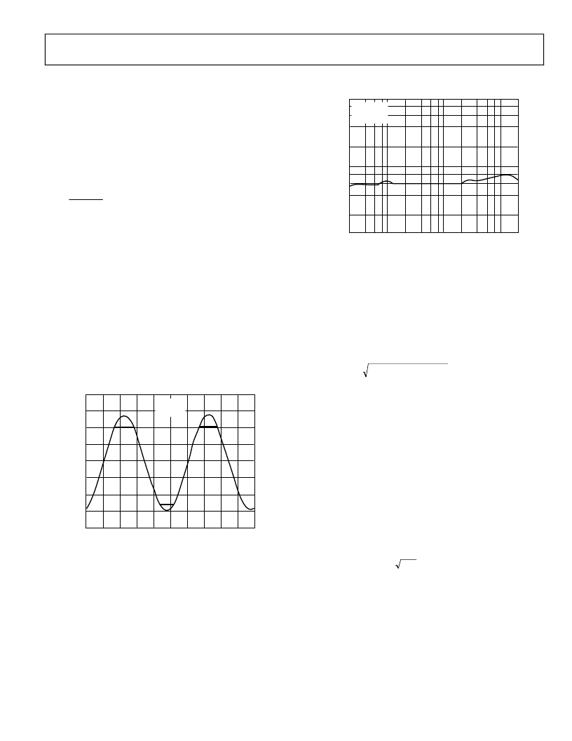
THD + NOISE
The AD8510/AD8512/AD8513 have low total harmonic distor-
tion and excellent gain linearity, making these amplifiers a great
choice for precision circuits with high closed-loop gain, and for
audio application circuits. Figure 42 shows that the AD8510/
AD8512/AD8513 have approximately 0.0005% of total distor-
tion when configured in positive unity gain (the worst case) and
driving a 100 k load.
FREQUENCY (Hz)
D
0
0.01
0.001
0.000120
100
1k
20k
V
SY
= ±5V
R
= 100k
BW = 22kHz
Figure 42. THD + N vs. Frequency
TOTAL NOISE INCLUDING SOURCE RESISTORS
The low input current noise and input bias current of the
AD8510/AD8512/AD8513 make them the ideal amplifiers for
circuits with substantial input source resistance. Input offset
voltage increases by less than 15 nV per 500 of source
resistance at room temperature. The total noise density of the
circuit is
(
)
S
S
n
n
nTOTAL
kTR
R
i
e
e
4
2
2
+
+
=
where:
e
n
is the input voltage noise density of the parts.
i
n
is the input current noise density of the parts.
R
S
is the source resistance at the noninverting terminal.
k
is Boltzman’s constant (1.38 × 10
–23
J/K).
T
is the ambient temperature in Kelvin (T = 273 + °C).
For
R
S
< 3.9 k,
e
n
dominates and
e
nTOTAL
≈
e
n
.
The current noise of the AD8510/AD8512/AD8513 is so low
that its total density does not become a significant term unless
R
S
is greater than 165 M, an impractical value for most
applications.
The total equivalent rms noise over a specific bandwidth is
expressed as
BW
e
e
nTOTAL
nTOTAL
=
where
BW
is the bandwidth in Hertz.
Note that the above analysis is valid for frequencies larger than
150 Hz and assumes flat noise above 10 kHz. For lower frequen-
cies, flicker noise (1/f) must be considered.
相关PDF资料 |
PDF描述 |
|---|---|
| AD8512AR | Precision, Very Low Noise, Low Input Bias Current, Wide Bandwidth JFET Operational Amplifiers |
| AD8512AR-REEL | Precision, Very Low Noise, Low Input Bias Current, Wide Bandwidth JFET Operational Amplifiers |
| AD8510ARZ-REEL | Precision, Very Low Noise, Low Input Bias Current, Wide Bandwidth JFET Operational Amplifiers |
| AD8522 | +5 Volt, Serial Input,Dual 12-Bit DAC(串行输入,双12位D/A转换器) |
| AD8531AKS | Precision, Quad, SPST Analog Switches |
相关代理商/技术参数 |
参数描述 |
|---|---|
| AD85-12/883B | 制造商:Analog 功能描述:_ |
| AD8512883B | 制造商:Analog 功能描述:_ |
| AD8512AR | 功能描述:IC OPAMP JFET 8MHZ DUAL LN 8SOIC RoHS:否 类别:集成电路 (IC) >> Linear - Amplifiers - Instrumentation 系列:- 标准包装:1 系列:- 放大器类型:通用 电路数:4 输出类型:满摆幅 转换速率:0.6 V/µs 增益带宽积:1MHz -3db带宽:- 电流 - 输入偏压:2pA 电压 - 输入偏移:1000µV 电流 - 电源:85µA 电流 - 输出 / 通道:20mA 电压 - 电源,单路/双路(±):1.8 V ~ 6 V 工作温度:-40°C ~ 125°C 安装类型:表面贴装 封装/外壳:14-SOIC(0.154",3.90mm 宽) 供应商设备封装:14-SOICN 包装:剪切带 (CT) 产品目录页面:680 (CN2011-ZH PDF) 其它名称:MCP6L04T-E/SLCT |
| AD8512ARM-R2 | 制造商:Analog Devices 功能描述:OP Amp Dual GP 制造商:Analog Devices 功能描述:IC AMP LOW NOISE |
| AD8512ARM-REEL | 制造商:Analog Devices 功能描述:OP AMP DUAL GP 15V 8MSOP - Tape and Reel 制造商:Analog Devices 功能描述:IC AMP LOW NOISE |
发布紧急采购,3分钟左右您将得到回复。