- 您现在的位置:买卖IC网 > PDF目录373947 > AD8512 (Analog Devices, Inc.) Precision, Very Low Noise, Low Input Bias Current, Wide Bandwidth JFET Operational Amplifiers PDF资料下载
参数资料
| 型号: | AD8512 |
| 厂商: | Analog Devices, Inc. |
| 英文描述: | Precision, Very Low Noise, Low Input Bias Current, Wide Bandwidth JFET Operational Amplifiers |
| 中文描述: | 精密,非常低噪声,低输入偏置电流,高带宽结型场效应管运算放大器 |
| 文件页数: | 15/20页 |
| 文件大小: | 497K |
| 代理商: | AD8512 |
AD8510/AD8512/AD8513
Rev. E | Page 15 of 20
TIME (1
μ
s/DIV)
V
V
SY
= ±15V
C
L
= 500pF
R
L
=10k
0
Figure 46. Capacitive Load Drive without Snubber
When the snubber circuit is used, the overshoot is reduced from
55% to less than 3% with the same load capacitance. Ringing is
virtually eliminated, as shown in Figure 47.
TIME (1
μ
s/DIV)
V
V
SY
= ±15V
R
L
=10k
C
L
= 500pF
R
S
=100
C
S
=1nF
0
Figure 47. Capacitive Load with Snubber Network
Optimum values for R
S
and C
S
depend on the load capacitance
and input stray capacitance and are determined empirically.
Table 5 shows a few values that can be used as starting points.
Table 5. Optimum Values for Capacitive Loads
C
LOAD
R
S
()
500 pF
100
2 nF
70
5 nF
60
C
S
1 nF
100 pF
300 pF
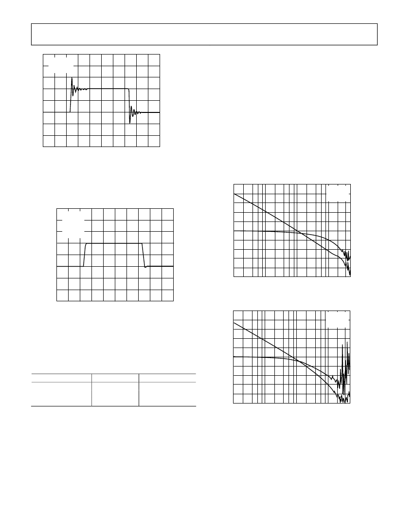
OPEN-LOOP GAIN AND PHASE RESPONSE
In addition to their impressive low noise, low offset voltage, and
offset current, the AD8510/AD8512/AD8513 have excellent
loop gain and phase response even when driving large resistive
and capacitive loads. They were compared to the OPA2132
under the same conditions. With a 2.5 k load at the output, the
AD8510/AD8512/AD8513 have more than 8 MHz of band-
width and a phase margin of more than 52°.
The OPA2132, on the other hand, has only 4.5 MHz of band-
width and 28° of phase margin under the same test conditions.
Even with a 1 nF capacitive load in parallel with the 2 k load
at the output, the AD8510/AD8512/AD8513 show much better
response than the OPA2132, whose phase margin is degraded to
less than 0, indicating oscillation.
FREQUENCY (Hz)
G
10k
–30
–20
–10
100k
0
10
30
1M
10M
50M
40
50
20
60
70
–135
–90
–45
0
45
90
135
190
225
270
315
P
V
SY
= ±15
V
R
L
= 2.5k
C
L
= 0
0
Figure 48. Frequency Response of the AD8510/AD8512/AD8513
FREQUENCY (Hz)
G
10k
–30
–20
–10
100k
0
10
30
1M
10M
50M
40
50
20
60
70
–135
–90
–45
0
45
90
135
190
225
270
315
P
V
SY
= ±15
V
R
L
= 2.5k
C
L
= 0
0
Figure 49. Frequency Response of the OPA2132
相关PDF资料 |
PDF描述 |
|---|---|
| AD8512AR | Precision, Very Low Noise, Low Input Bias Current, Wide Bandwidth JFET Operational Amplifiers |
| AD8512AR-REEL | Precision, Very Low Noise, Low Input Bias Current, Wide Bandwidth JFET Operational Amplifiers |
| AD8510ARZ-REEL | Precision, Very Low Noise, Low Input Bias Current, Wide Bandwidth JFET Operational Amplifiers |
| AD8522 | +5 Volt, Serial Input,Dual 12-Bit DAC(串行输入,双12位D/A转换器) |
| AD8531AKS | Precision, Quad, SPST Analog Switches |
相关代理商/技术参数 |
参数描述 |
|---|---|
| AD85-12/883B | 制造商:Analog 功能描述:_ |
| AD8512883B | 制造商:Analog 功能描述:_ |
| AD8512AR | 功能描述:IC OPAMP JFET 8MHZ DUAL LN 8SOIC RoHS:否 类别:集成电路 (IC) >> Linear - Amplifiers - Instrumentation 系列:- 标准包装:1 系列:- 放大器类型:通用 电路数:4 输出类型:满摆幅 转换速率:0.6 V/µs 增益带宽积:1MHz -3db带宽:- 电流 - 输入偏压:2pA 电压 - 输入偏移:1000µV 电流 - 电源:85µA 电流 - 输出 / 通道:20mA 电压 - 电源,单路/双路(±):1.8 V ~ 6 V 工作温度:-40°C ~ 125°C 安装类型:表面贴装 封装/外壳:14-SOIC(0.154",3.90mm 宽) 供应商设备封装:14-SOICN 包装:剪切带 (CT) 产品目录页面:680 (CN2011-ZH PDF) 其它名称:MCP6L04T-E/SLCT |
| AD8512ARM-R2 | 制造商:Analog Devices 功能描述:OP Amp Dual GP 制造商:Analog Devices 功能描述:IC AMP LOW NOISE |
| AD8512ARM-REEL | 制造商:Analog Devices 功能描述:OP AMP DUAL GP 15V 8MSOP - Tape and Reel 制造商:Analog Devices 功能描述:IC AMP LOW NOISE |
发布紧急采购,3分钟左右您将得到回复。