- 您现在的位置:买卖IC网 > PDF目录373947 > AD8522 (Analog Devices, Inc.) +5 Volt, Serial Input,Dual 12-Bit DAC(串行输入,双12位D/A转换器) PDF资料下载
参数资料
| 型号: | AD8522 |
| 厂商: | Analog Devices, Inc. |
| 英文描述: | +5 Volt, Serial Input,Dual 12-Bit DAC(串行输入,双12位D/A转换器) |
| 中文描述: | 5伏,串行输入,双12位DAC(串行输入,双12位的D / A转换器) |
| 文件页数: | 4/8页 |
| 文件大小: | 189K |
| 代理商: | AD8522 |
AD8522
–4–
REV. A
ABSOLUT E MAX IMUM RAT INGS*
V
DD
to DGND & AGND . . . . . . . . . . . . . . . . . . . –0.3 V, +7 V
Logic Inputs and Output to DGND . . . . .–0.3 V, V
DD
+ 0.3 V
V
OUT
to AGND . . . . . . . . . . . . . . . . . . . . .–0.3 V, V
DD
+ 0.3 V
V
REF
to AGND . . . . . . . . . . . . . . . . . . . . .–0.3 V, V
DD
+ 0.3 V
AGND to DGND . . . . . . . . . . . . . . . . . . . . . . . . . –0.3 V, V
DD
I
OUT
Short Circuit to GND or V
DD
. . . . . . . . . . . . . . . . 50 mA
Package Power Dissipation . . . . . . . . . . . . . . .(T
J
max–T
A
)/
θ
JA
T hermal Resistance,
θ
JA
14-Pin Plastic DIP Package (N-14) . . . . . . . . . . . . . 83
°
C/W
14-Lead SOIC Package (SO-14) . . . . . . . . . . . . . . 120
°
C/W
Maximum Junction T emperature (T
J
max) . . . . . . . . . . 150
°
C
Operating T emperature Range . . . . . . . . . . . . .–40
°
C to +85
°
C
Storage T emperature Range . . . . . . . . . . . . .–65
°
C to +150
°
C
Lead T emperature (Soldering, 10 sec) . . . . . . . . . . . . . +300
°
C
*Stresses above those listed under “Absolute Maximum Ratings” may cause
permanent damage to the device. T his is a stress rating only and functional
operation of the device at these or any other conditions above those indicated in the
operational sections of this specification is not implied. Exposure to absolute
maximum rating conditions for extended periods may affect device reliability.
ORDE RING GUIDE
T emperature
Range
Package
Description
Package
Option
Model
AD8522AN
AD8522AR
–40
°
C to +85
°
C
–40
°
C to +85
°
C
14-Pin P-DIP
14-Lead SOIC
N-14
SO-14
T he AD8522 contains 1482 transistors.
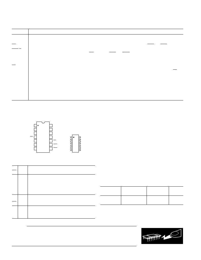
PIN CONFIGURAT ION
14-Pin Plastic DIP 14-Lead SO-14
V
OUTA
AGND
V
OUTB
V
REF
CLK
SDI
SDO
RS
LDA
LDB
DGND
CS
V
DD
MSB
1
2
14
13
10
9
8
12
11
5
6
7
3
4
(Not To Scale)
1
T able II. T ruth T ables
DAC Register Preset
Register Activity
RS
MSB
0
0
Asynchronously Resets DAC Registers to Zero
Scale
Asynchronously Presets DAC Registers to
Half Scale (800
H
)
None
0
1
1
X
Shift Register
CS
CLK
Shift Register
1
0
X
↑
No Effect
Shifts Register One Bit, SDO Outputs Data
from 16 Clocks Earlier
WARNING!
ESD SENSITIVE DEVICE
C AUT ION
ESD (electrostatic discharge) sensitive device. Electrostatic charges as high as 4000 V readily
accumulate on the human body and test equipment and can discharge without detection.
Although the AD8522 features proprietary ESD protection circuitry, permanent damage may
occur on devices subjected to high energy electrostatic discharges. T herefore, proper ESD
precautions are recommended to avoid performance degradation or loss of functionality.
PIN DE SCRIPT ION
Pin
Function
SDI
CLK
CS
LDA
/
B
Serial Data Input, input data loads directly into the shift register.
Clock input, positive edge clocks data into shift register.
Chip Select, active low input. Prevents shift register loading when high. Does not affect
LDA
and
LDB
operation.
Load DAC register strobes, active low. T ransfers shift register data to DAC register. See truth table for operation.
Software decode feature only requires one
LD
strobe. T ie
LDA
and
LDB
together or use one of them with the
other pin tied high.
Serial Data Output. Output of shift register, always active.
Resets DAC registers to condition determined by MSB pin. Active low input.
Digital input: High presets DAC registers to half scale (800
H
); Low clears all registers to zero (000
H
), when
RS
is
strobed to active low.
Positive +5 V power supply input. T olerance
±
10%.
Analog Ground Input.
Digital Ground Input.
Reference Voltage Output, 2.5 V nominal.
DAC A/B voltage outputs, 4.095 V full scale,
±
5 mA output.
SDO
RS
MSB
V
DD
AGND
DGND
V
REF
V
OUT A/B
相关PDF资料 |
PDF描述 |
|---|---|
| AD8531AKS | Precision, Quad, SPST Analog Switches |
| AD8531AR | Low Cost, 250 mA Output Single-Supply Amplifiers |
| AD8531ART | Low Cost, 250 mA Output Single-Supply Amplifiers |
| AD8531 | Low Cost, 250 mA Output Single-Supply Amplifiers(低成本,250mA输出,单电源放大器) |
| AD8532 | Low Cost, 250 mA Output Single-Supply Amplifiers(低成本,250mA输出,单电源双放大器) |
相关代理商/技术参数 |
参数描述 |
|---|---|
| AD8522ACPZ-REEL | 功能描述:IC DAC DUAL 12BIT 5V 制造商:analog devices inc. 系列:- 零件状态:上次购买时间 标准包装:1 |
| AD8522ACPZ-REEL7 | 功能描述:IC DAC DUAL 12BIT 5V 制造商:analog devices inc. 系列:- 零件状态:上次购买时间 标准包装:1 |
| AD8522AN | 功能描述:IC DAC DUAL 12BIT 5V 14-DIP RoHS:否 类别:集成电路 (IC) >> 数据采集 - 数模转换器 系列:- 产品培训模块:Data Converter Fundamentals DAC Architectures 标准包装:750 系列:- 设置时间:7µs 位数:16 数据接口:并联 转换器数目:1 电压电源:双 ± 功率耗散(最大):100mW 工作温度:0°C ~ 70°C 安装类型:表面贴装 封装/外壳:28-LCC(J 形引线) 供应商设备封装:28-PLCC(11.51x11.51) 包装:带卷 (TR) 输出数目和类型:1 电压,单极;1 电压,双极 采样率(每秒):143k |
| AD8522AN | 制造商:Analog Devices 功能描述:SEMICONDUCTORSLINEAR |
| AD8522ANZ | 功能描述:IC DAC DUAL 12BIT 5V 14DIP RoHS:是 类别:集成电路 (IC) >> 数据采集 - 数模转换器 系列:- 产品培训模块:Data Converter Fundamentals DAC Architectures 标准包装:750 系列:- 设置时间:7µs 位数:16 数据接口:并联 转换器数目:1 电压电源:双 ± 功率耗散(最大):100mW 工作温度:0°C ~ 70°C 安装类型:表面贴装 封装/外壳:28-LCC(J 形引线) 供应商设备封装:28-PLCC(11.51x11.51) 包装:带卷 (TR) 输出数目和类型:1 电压,单极;1 电压,双极 采样率(每秒):143k |
发布紧急采购,3分钟左右您将得到回复。