- 您现在的位置:买卖IC网 > PDF目录373947 > AD8522 (Analog Devices, Inc.) +5 Volt, Serial Input,Dual 12-Bit DAC(串行输入,双12位D/A转换器) PDF资料下载
参数资料
| 型号: | AD8522 |
| 厂商: | Analog Devices, Inc. |
| 英文描述: | +5 Volt, Serial Input,Dual 12-Bit DAC(串行输入,双12位D/A转换器) |
| 中文描述: | 5伏,串行输入,双12位DAC(串行输入,双12位的D / A转换器) |
| 文件页数: | 6/8页 |
| 文件大小: | 189K |
| 代理商: | AD8522 |
AD8522
input register and transferring the 12 bits of data into the de-
coded address determined by the address bits A and B in the se-
rial input register.
Unipolar Output Operation
T his is the basic mode of operation for the AD8522. T he
AD8522 has been designed to drive loads as low as 820
in
parallel with 500 pF. T he code table for this operation is shown
in T able III.
T able III. Unipolar Code T able
Hexadecimal
Number in
DAC Register
Decimal
Number in
DAC Register
Analog
Output
Voltage (V)
FFF
801
800
7FF
000
4095
2049
2048
2047
0
+4.095
+2.049
+2.048
+2.047
0
5
2
0
1
3
4
10
100
100k
10k
1k
R
TIED TO AGND
DATA = FFF
H
V
DD
= +5V
T
A
= +25
°
C
R
TIED TO +5V
DATA = 000
H
LOAD RESISTANCE –
O
V
IN
H = +5V
V
IN
L = 0V
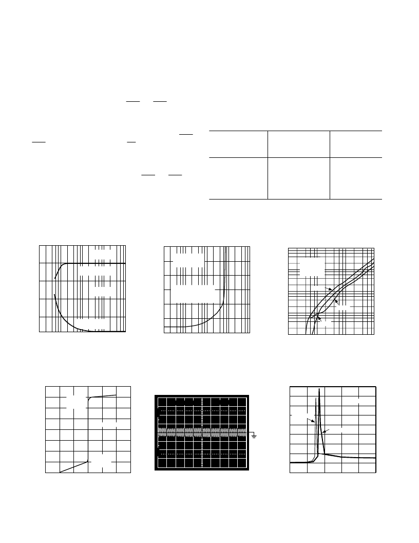
Figure 6. Output Swing vs. Load
80
60
40
20
0
–20
–40
–60
–80
1
2
3
OUTPUT VOLTAGE – Volts
O
DATA = 800
H
POSITIVE
CURRENT
LIMIT
NEGATIVE
CURRENT
LIMIT
Figure 9. I
OUT
vs. V
OUT
5.2
5.0
4.8
4.6
4.4
4.2
4.0
0.01
0.1
100
10
1.0
OUTPUT LOAD CURRENT – mA
V
D
V
≤
1 LSB
DATA = FFF
H
T
A
= +25
°
C
PROPER OPERATION
WHEN V
SUPPLY
VOLTAGE IS ABOVE
CURVE
Figure 7. Minimum Supply Voltage
vs. Load Current
100
90
10
0%
2
100μs/DIV
T
A
= +25
°
C
NBW = 1MHz
Figure 10. Broadband Noise
1
10
1000
100
100
1
0.1
10
0.01
+85
°
C
–55
°
C
+25
°
C
V
= +5V
DATA = 000
H
V
IH
= 5.0V
V
IL
= 0.0V
OUTPUT SINK CURRENT – μA
O
Figure 8. Pull-Down Voltage vs. Out-
put Sink Current Capability
9
8
7
6
5
4
3
2
1
0
0
1
3
4
5
2
V
DD
= +4.5V
V
DD
= +5V
T
A
= +25
°
C
S
D
LOGIC INPUT VOLTAGE V
IN
H – Volts
Figure 11. Supply Current vs. Logic
Input Voltage
Typical Performance Characteristics
is possible down to +4.3 V. T he minimum operating supply
voltage versus load current plot, in Figure 7, provides informa-
tion for operation below V
DD
= +4.5 V.
T IMING AND CONT ROL
T he AD8522 has a 16-bit serial input register that accepts
clocked in data when the CS pin is active low. T he DAC regis-
ters are updated by the Load Enable (
LDA
and
LDB
) pins.
T he AD8522 offers two modes of data loading. T he first mode,
hardware-load, directs the data currently clocked into the serial
shift register into either the DAC A or the DAC B register or
both depending on the external active low strobing of the
LDA
or
LDB
pin. Serial data register bit Sf/
Hd
must be low for this
mode to be in effect.
T he second mode of operation is software-load which is de-
signed to minimize the number of control lines connected to
the AD8522. In this mode of operation the
LDA
and
LDB
pins
act as one control input taking the present contents of the serial
–6–
REV. A
相关PDF资料 |
PDF描述 |
|---|---|
| AD8531AKS | Precision, Quad, SPST Analog Switches |
| AD8531AR | Low Cost, 250 mA Output Single-Supply Amplifiers |
| AD8531ART | Low Cost, 250 mA Output Single-Supply Amplifiers |
| AD8531 | Low Cost, 250 mA Output Single-Supply Amplifiers(低成本,250mA输出,单电源放大器) |
| AD8532 | Low Cost, 250 mA Output Single-Supply Amplifiers(低成本,250mA输出,单电源双放大器) |
相关代理商/技术参数 |
参数描述 |
|---|---|
| AD8522ACPZ-REEL | 功能描述:IC DAC DUAL 12BIT 5V 制造商:analog devices inc. 系列:- 零件状态:上次购买时间 标准包装:1 |
| AD8522ACPZ-REEL7 | 功能描述:IC DAC DUAL 12BIT 5V 制造商:analog devices inc. 系列:- 零件状态:上次购买时间 标准包装:1 |
| AD8522AN | 功能描述:IC DAC DUAL 12BIT 5V 14-DIP RoHS:否 类别:集成电路 (IC) >> 数据采集 - 数模转换器 系列:- 产品培训模块:Data Converter Fundamentals DAC Architectures 标准包装:750 系列:- 设置时间:7µs 位数:16 数据接口:并联 转换器数目:1 电压电源:双 ± 功率耗散(最大):100mW 工作温度:0°C ~ 70°C 安装类型:表面贴装 封装/外壳:28-LCC(J 形引线) 供应商设备封装:28-PLCC(11.51x11.51) 包装:带卷 (TR) 输出数目和类型:1 电压,单极;1 电压,双极 采样率(每秒):143k |
| AD8522AN | 制造商:Analog Devices 功能描述:SEMICONDUCTORSLINEAR |
| AD8522ANZ | 功能描述:IC DAC DUAL 12BIT 5V 14DIP RoHS:是 类别:集成电路 (IC) >> 数据采集 - 数模转换器 系列:- 产品培训模块:Data Converter Fundamentals DAC Architectures 标准包装:750 系列:- 设置时间:7µs 位数:16 数据接口:并联 转换器数目:1 电压电源:双 ± 功率耗散(最大):100mW 工作温度:0°C ~ 70°C 安装类型:表面贴装 封装/外壳:28-LCC(J 形引线) 供应商设备封装:28-PLCC(11.51x11.51) 包装:带卷 (TR) 输出数目和类型:1 电压,单极;1 电压,双极 采样率(每秒):143k |
发布紧急采购,3分钟左右您将得到回复。