- 您现在的位置:买卖IC网 > PDF目录373947 > AD8531AR (ANALOG DEVICES INC) Low Cost, 250 mA Output Single-Supply Amplifiers PDF资料下载
参数资料
| 型号: | AD8531AR |
| 厂商: | ANALOG DEVICES INC |
| 元件分类: | 运动控制电子 |
| 英文描述: | Low Cost, 250 mA Output Single-Supply Amplifiers |
| 中文描述: | OP-AMP, 30000 uV OFFSET-MAX, 2.2 MHz BAND WIDTH, PDSO8 |
| 封装: | MS-012AA, SOIC-8 |
| 文件页数: | 8/16页 |
| 文件大小: | 417K |
| 代理商: | AD8531AR |
AD8531/AD8532/AD8534
REV. D
–8–
100
90
10
0%
V
S
= 2.5V
A
V
= 1
R
L
= 2k
T
A
= 25 C
500mV
500ns
Figure 29. Large Signal Transient
Response
APPLICATIONS
THEORY OF OPERATION
The AD8531/AD8532/AD8534 is an all-CMOS, high output
current drive, rail-to-rail input/output operational amplifier.
This is the latest entry in Analog Devices’ expanding family of
single-supply devices for the multimedia and telecom market-
places. Its high output current drive and stability with heavy
capacitive loads makes the AD8531/AD8532/AD8534 an excel-
lent choice as a drive amplifier for LCD panels.
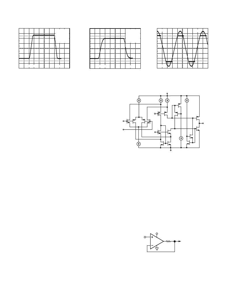
Figure 32 illustrates a simplified equivalent circuit for the AD8531/
AD8532/AD8534. Like many rail-to-rail input amplifier configu-
rations, it is comprised of two differential pairs, one n-channel
(M1–M2) and one p-channel (M3–M4). These differential pairs
are biased by 50
m
A current sources, each with a compliance
limit of approximately 0.5 V from either supply voltage rail. The
differential input voltage is then converted into a pair of differ-
ential output currents. These differential output currents are
then combined in a compound folded-cascade second gain
stage (M5–M9). The outputs of the second gain stage at M8
and M9 provide the gate voltage drive to the rail-to-rail output
stage. Additional signal current recombination for the output
stage is achieved through the use of transistors M11–M14.
In order to achieve rail-to-rail output swings, the AD8531/
AD8532/AD8534 design employs a complementary common-
source output stage (M15–M16). However, the output voltage
swing is directly dependent on the load current, as the difference
between the output voltage and the supply is determined by the
AD8531/AD8532/AD8534’s output transistors on-channel
resistance (see Figures 8 and 9). The output stage also exhibits
voltage gain by virtue of the use of common-source amplifiers;
as a result, the voltage gain of the output stage (thus, the open-
loop gain of the device) exhibits a strong dependence to the total
load resistance at the output of the AD8531/AD8532/AD8534.
50 A
100 A
100 A
20 A
V
B2
M5
M8
M12
M15
M16
M11
OUT
M3
M4
M2
M1
IN–
IN+
V
B3
M6
M7
M10
20 A
M13
50 A
V+
V–
M9
M14
Figure 32. AD8531/AD8532/AD8534 Simplified Equivalent
Circuit
Short-Circuit Protection
As a result of the design of the output stage for maximum load
current capability, the AD8531/AD8532/AD8534 does not have
any internal short-circuit protection circuitry. Direct connection of
the AD8531/AD8532/AD8534’s output to the positive supply
in single-supply applications will destroy the device. In those
applications where some protection is needed, but not at the
expense of reduced output voltage headroom, a low value resis-
tor in series with the output, as shown in Figure 33, can be
used. The resistor, connected within the feedback loop of the
amplifier, will have very little effect on the performance of the
amplifier other than limiting the maximum available output volt-
age swing. For single 5 V supply applications, resistors less than
20
W
are not recommended.
5V
R
X
20
V
OUT
V
IN
AD8532
Figure 33. Output Short-Circuit Protection
V
S
= 1.35V
A
V
= 1
R
L
= 2k
T
A
= 25 C
500ns
500mV
100
90
10
0%
Figure 30. Large Signal Transient
Response
1V
10 s
1V
0%
10
90
100
Figure 31. No Phase Reversal
相关PDF资料 |
PDF描述 |
|---|---|
| AD8531ART | Low Cost, 250 mA Output Single-Supply Amplifiers |
| AD8531 | Low Cost, 250 mA Output Single-Supply Amplifiers(低成本,250mA输出,单电源放大器) |
| AD8532 | Low Cost, 250 mA Output Single-Supply Amplifiers(低成本,250mA输出,单电源双放大器) |
| AD8534 | Low Cost, 250 mA Output Single-Supply Amplifiers(低成本,250mA输出,单电源四放大器) |
| AD8538_07 | Low Power, Precision, Auto-Zero Op Amps |
相关代理商/技术参数 |
参数描述 |
|---|---|
| AD8531AR-REEL | 制造商:Analog Devices 功能描述:OP Amp Single GP R-R I/O 6V 8-Pin SOIC N T/R |
| AD8531ART | 制造商:AD 制造商全称:Analog Devices 功能描述:Low Cost, 250 mA Output Single-Supply Amplifiers |
| AD8531ART-REEL | 制造商:Analog Devices 功能描述:OP Amp Single GP R-R I/O 6V 5-Pin SOT-23 T/R 制造商:Rochester Electronics LLC 功能描述:SINGLE 250MA RAIL TO RAIL OP AMP - Tape and Reel |
| AD8531ART-REEL7 | 制造商:Analog Devices 功能描述:OP Amp Single GP R-R I/O 6V 5-Pin SOT-23 T/R 制造商:Rochester Electronics LLC 功能描述:SINGLE 250MA RAIL TO RAIL OP AMP - Tape and Reel |
| AD8531ARTZ-REEL | 功能描述:IC OPAMP GP R-R CMOS SOT23-5 RoHS:是 类别:集成电路 (IC) >> Linear - Amplifiers - Instrumentation 系列:- 标准包装:160 系列:- 放大器类型:通用 电路数:4 输出类型:满摆幅 转换速率:10 V/µs 增益带宽积:9MHz -3db带宽:- 电流 - 输入偏压:1pA 电压 - 输入偏移:250µV 电流 - 电源:730µA 电流 - 输出 / 通道:28mA 电压 - 电源,单路/双路(±):2.7 V ~ 5.5 V,±1.35 V ~ 2.75 V 工作温度:-40°C ~ 125°C 安装类型:表面贴装 封装/外壳:16-SOIC(0.154",3.90mm 宽) 供应商设备封装:16-SOIC N 包装:管件 |
发布紧急采购,3分钟左右您将得到回复。