参数资料
| 型号: | AD8582AN |
| 厂商: | Analog Devices Inc |
| 文件页数: | 3/8页 |
| 文件大小: | 0K |
| 描述: | IC DAC DUAL 12BIT 5V 24-DIP |
| 产品培训模块: | Data Converter Fundamentals DAC Architectures |
| 标准包装: | 15 |
| 设置时间: | 16µs |
| 位数: | 12 |
| 数据接口: | 并联 |
| 转换器数目: | 2 |
| 电压电源: | 单电源 |
| 功率耗散(最大): | 35mW |
| 工作温度: | -40°C ~ 85°C |
| 安装类型: | 通孔 |
| 封装/外壳: | 24-DIP(0.300",7.62mm) |
| 供应商设备封装: | 24-PDIP |
| 包装: | 管件 |
| 输出数目和类型: | 2 电压,单极 |
| 采样率(每秒): | 62.5k |
–3–
REV. 0
AD8582
WARNING!
ESD SENSITIVE DEVICE
CAUTION
ESD (electrostatic discharge) sensitive device. Electrostatic charges as high as 4000 V readily
accumulate on the human body and test equipment and can discharge without detection.
Although the AD8582 features proprietary ESD protection circuitry, permanent damage may
occur on devices subjected to high energy electrostatic discharges. Therefore, proper ESD
precautions are recommended to avoid performance degradation or loss of functionality.
ABSOLUTE MAXIMUM RATINGS*
VDD to DGND & AGND . . . . . . . . . . . . . . . . . . . –0.3 V, +7 V
Logic Inputs to DGND . . . . . . . . . . . . . . . –0.3 V, VDD + 0.3 V
VOUT to AGND . . . . . . . . . . . . . . . . . . . . . –0.3 V, VDD + 0.3 V
VREF to AGND . . . . . . . . . . . . . . . . . . . . . –0.3 V, VDD + 0.3 V
AGND to DGND . . . . . . . . . . . . . . . . . . . . . . . . . –0.3 V, VDD
IOUT Short Circuit to GND . . . . . . . . . . . . . . . . . . . . . . 50 mA
Package Power Dissipation . . . . . . . . . . . . . . . (TJ max–TA)/θJA
Thermal Resistance,
θ
JA
24-Pin Plastic DIP Package (N-24) . . . . . . . . . . . . . 62
°C/W
24-Lead SOIC Package (SOL-24) . . . . . . . . . . . . . . 73
°C/W
Maximum Junction Temperature (TJ max) . . . . . . . . . . 150
°C
Operating Temperature Range . . . . . . . . . . . . . –40
°C to +85°C
Storage Temperature Range . . . . . . . . . . . . . –65
°C to +150°C
Lead Temperature (Soldering, 10 sec) . . . . . . . . . . . . . +300
°C
*Stresses above those listed under “Absolute Maximum Ratings” may cause
permanent damage to the device. This is a stress rating only and functional
operation of the device at these or any other conditions above those indicated in the
operational sections of this specification is not implied. Exposure to absolute
maximum rating conditions for extended periods may affect device reliability.
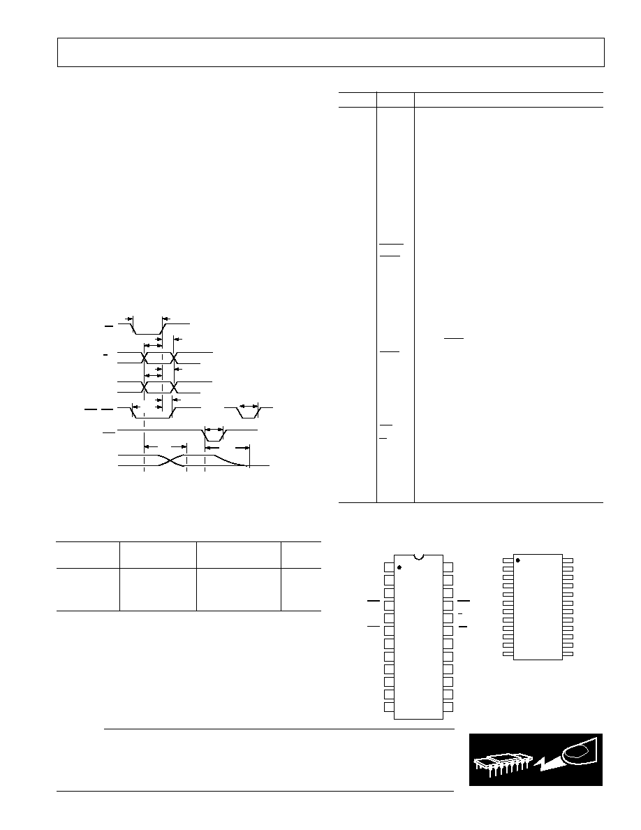
PIN DESCRIPTION
Pin No.
Name
Description
1, 24
VOUTA
Voltage outputs from the DACs. Fixed
VOUTB
output voltage range of 0 V to 4.095 V
with 1 mV/LSB. An internal
temperature stabilized reference
maintains a fixed full-scale voltage
independent of time, temperature and
power supply variations.
2
AGND
Analog Ground. Ground reference for
the internal bandgap reference voltage,
the DAC, and the output buffer.
3
DGND
Digital ground for input logic.
4, 21
LDA,
Load DAC register strobes. Transfers
LDB
input register data to the DAC registers.
Active low inputs, Level sensitive latch.
May be connected together to double-
buffer load DAC registers.
5
MSB
Digital Input: High presets DAC
registers to half scale (800H), Low
clears DAC registers to zero (000H)
upon RST assertion.
6
RST
Active low digital input that clears the
DAC register to zero, setting the DAC
to minimum scale when MSB pin = 0,
or half-scale when MSB pin = 1.
7–18
DB0–11
Twelve Binary Data Bit Inputs. DB11 is
the MSB and DB0 is the LSB.
19
CS
Chip Select. Active low input.
20
A
/B
Select DAC A = 0 or DAC B = 1.
22
VDD
Positive Supply. Nominal value +5 V,
±5%.
23
VREF
Nominal 2.5 V reference output
voltage. This node must be buffered if
required to drive external loads.
PIN CONFIGURATIONS
N-24
24-Pin Plastic DIP
SOL-24
24-Pin SOIC
VOUTA
AGND
VOUTB
VREF
MSB
DB0
DB11
DGND
VDD
DB1
DB10
DB2
DB9
DB3
DB8
DB4
DB7
DB5
DB6
14
1
2
24
23
5
6
7
20
19
18
3
4
22
21
8
17
9
16
10
15
11
TOP VIEW
(Not to Scale)
12
13
AD8582
LDA
RST
LDB
CS
A/B
TOP VIEW
(Not to Scale)
12
13
AD8582
1
24
LDA, LDB
CS
A/B
D0–D11
RST
t
AS
t
AH
t
DS
t
DH
t
LDW
t
RSW
t
LS
t
LH
VOUT
t
S
t
S
± 1LSB
ERROR BAND
t
CSW
Timing Diagram
ORDERING INFORMATION*
Temperature
Package
Model
Range
Description
Option
AD8582AN
–40
°C to +85°C 24-Pin Plastic DIP N-24
AD8582AR
–40
°C to +85°C 24-Lead SOIC
SOL-24
AD8582Chips
+25
°C
Die
*For die specifications contact your local Analog Devices sales office. The
AD8582 contains 1270 transistors.
相关PDF资料 |
PDF描述 |
|---|---|
| AD8600APZ-REEL | IC DAC MULT 16CH 8BIT 44PLCC |
| AD872AJD | IC ADC 12BIT 10MSPS 28-CDIP |
| AD876JSTZ | IC ADC 10BIT 20MSPS CMOS 48TQFP |
| AD8802AR | IC DAC 8BIT 12CH W/SD 20-SOIC |
| AD8803AR | IC DAC 8BIT OCTAL W/SD 16-SOIC |
相关代理商/技术参数 |
参数描述 |
|---|---|
| AD8582ANZ | 功能描述:IC DAC DUAL 12BIT 5V 24DIP RoHS:是 类别:集成电路 (IC) >> 数据采集 - 数模转换器 系列:- 标准包装:1 系列:- 设置时间:4.5µs 位数:12 数据接口:串行,SPI? 转换器数目:1 电压电源:单电源 功率耗散(最大):- 工作温度:-40°C ~ 125°C 安装类型:表面贴装 封装/外壳:8-SOIC(0.154",3.90mm 宽) 供应商设备封装:8-SOICN 包装:剪切带 (CT) 输出数目和类型:1 电压,单极;1 电压,双极 采样率(每秒):* 其它名称:MCP4921T-E/SNCTMCP4921T-E/SNRCTMCP4921T-E/SNRCT-ND |
| AD8582AR | 功能描述:IC DAC 12BIT DUAL 5V 24-SOIC RoHS:否 类别:集成电路 (IC) >> 数据采集 - 数模转换器 系列:- 产品培训模块:Data Converter Fundamentals DAC Architectures 标准包装:750 系列:- 设置时间:7µs 位数:16 数据接口:并联 转换器数目:1 电压电源:双 ± 功率耗散(最大):100mW 工作温度:0°C ~ 70°C 安装类型:表面贴装 封装/外壳:28-LCC(J 形引线) 供应商设备封装:28-PLCC(11.51x11.51) 包装:带卷 (TR) 输出数目和类型:1 电压,单极;1 电压,双极 采样率(每秒):143k |
| AD8582AR-REEL | 功能描述:IC DAC DUAL 12BIT 5V 24SOIC RoHS:否 类别:集成电路 (IC) >> 数据采集 - 数模转换器 系列:- 产品培训模块:Data Converter Fundamentals DAC Architectures 标准包装:750 系列:- 设置时间:7µs 位数:16 数据接口:并联 转换器数目:1 电压电源:双 ± 功率耗散(最大):100mW 工作温度:0°C ~ 70°C 安装类型:表面贴装 封装/外壳:28-LCC(J 形引线) 供应商设备封装:28-PLCC(11.51x11.51) 包装:带卷 (TR) 输出数目和类型:1 电压,单极;1 电压,双极 采样率(每秒):143k |
| AD8582ARZ | 功能描述:IC DAC 12BIT DUAL 5V 24-SOIC RoHS:是 类别:集成电路 (IC) >> 数据采集 - 数模转换器 系列:- 产品培训模块:Lead (SnPb) Finish for COTS Obsolescence Mitigation Program 标准包装:50 系列:- 设置时间:4µs 位数:12 数据接口:串行 转换器数目:2 电压电源:单电源 功率耗散(最大):- 工作温度:-40°C ~ 85°C 安装类型:表面贴装 封装/外壳:8-TSSOP,8-MSOP(0.118",3.00mm 宽) 供应商设备封装:8-uMAX 包装:管件 输出数目和类型:2 电压,单极 采样率(每秒):* 产品目录页面:1398 (CN2011-ZH PDF) |
| AD8582ARZ-REEL | 功能描述:IC DAC DUAL 12BIT 5V 24SOIC RoHS:是 类别:集成电路 (IC) >> 数据采集 - 数模转换器 系列:- 产品培训模块:Data Converter Fundamentals DAC Architectures 标准包装:750 系列:- 设置时间:7µs 位数:16 数据接口:并联 转换器数目:1 电压电源:双 ± 功率耗散(最大):100mW 工作温度:0°C ~ 70°C 安装类型:表面贴装 封装/外壳:28-LCC(J 形引线) 供应商设备封装:28-PLCC(11.51x11.51) 包装:带卷 (TR) 输出数目和类型:1 电压,单极;1 电压,双极 采样率(每秒):143k |
发布紧急采购,3分钟左右您将得到回复。