参数资料
| 型号: | AD8582AN |
| 厂商: | Analog Devices Inc |
| 文件页数: | 4/8页 |
| 文件大小: | 0K |
| 描述: | IC DAC DUAL 12BIT 5V 24-DIP |
| 产品培训模块: | Data Converter Fundamentals DAC Architectures |
| 标准包装: | 15 |
| 设置时间: | 16µs |
| 位数: | 12 |
| 数据接口: | 并联 |
| 转换器数目: | 2 |
| 电压电源: | 单电源 |
| 功率耗散(最大): | 35mW |
| 工作温度: | -40°C ~ 85°C |
| 安装类型: | 通孔 |
| 封装/外壳: | 24-DIP(0.300",7.62mm) |
| 供应商设备封装: | 24-PDIP |
| 包装: | 管件 |
| 输出数目和类型: | 2 电压,单极 |
| 采样率(每秒): | 62.5k |
REV. 0
–4–
AD8582
Table I. Control Logic Truth Table
CS
A
/B
LDA
LDB
RST
MSB
Input Register
DAC Register
L
HHHX
Write to A
Latched
L
HHHHX
Write to B
Latched
LLL
H
X
Write to A
A Transparent
L
H
L
H
X
Write to B
B Transparent
H
X
L
H
X
Latched
A & B Transparent
H
X
^
H
X
Latched
XXXXL
L
Reset to Zero Scale
XXXXL
H
Reset to Midscale
H
XXX^
X
Latch Reset Value
^Denotes positive edge triggered.
OPERATION
The AD8582 is a complete, ready-to-use dual 12-bit digital-to-
analog converter. Only one +5 V power supply is necessary for
operation. It contains two voltage-switched, 12-bit, laser-
trimmed digital-to-analog converters, a curvature-corrected
bandgap reference, rail-to-rail output op amps, input registers,
and DAC registers. The parallel data interface consists of twelve
data bits, DB0–DB11, an address select pin A/B, two load
strobe pins (LDA, LDB) and an active low CS strobe. In addi-
tion an asynchronous RST pin will set all DAC register bits to
zero causing the VOUT to become zero volts, or to midscale for
trimming applications when the MSB pin is programmed to
Logic 1. This function is useful for power on reset or system
failure recovery to a known state.
D/A CONVERTER SECTION
The internal DAC is a 12-bit voltage-mode device with an
output that swings from AGND potential to the 2.5 volt in-
ternal bandgap voltage. It uses a laser trimmed R-2R
ladder which is switched by N channel MOSFETs. The out-
put voltage of the DAC has a constant resistance independent
of digital input code. The DAC output (not available to the
user) is internally connected to the rail-to-rail output op amp.
AMPLIFIER SECTION
The internal DAC’s output is buffered by a low power con-
sumption precision amplifier. This low power amplifier contains
a differential PNP pair input stage which provides low offset
voltage and low noise, as well as the ability to amplify the zero-
scale DAC output voltages. The rail-to-rail amplifier is config-
ured in a gain of 1.6384 (= 4.095 V/2.5 V) in order to set the
4.095 volt full-scale output (1 mV/LSB). See Figure 3 for an
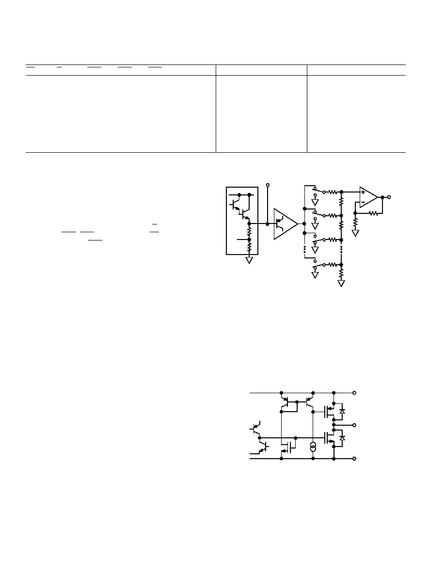
equivalent circuit schematic of the analog section.
The op amp has a 16
s typical settling time to 0.01%. There
are slight differences in settling time for negative slewing signals
versus positive. See the oscilloscope photos in the Typical Per-
formances section of this data sheet.
Figure 3. Equivalent Schematic of Analog Portion
R1
R2
VOUT
RAIL-TO-RAIL
OUTPUT
AMPLIFIER
R
BANDGAP
REFERENCE
VREF
2.5V
2R
R
2R
SPDT
N CH FET
SWITCHES
2R
AV = 4.095/2.5
= 1.638V/V
VOLTAGE SWITCHED 12-BIT
R-2R D/A CONVERTER
BUFFER
2R
OUTPUT SECTION
The rail-to-rail output stage of this amplifier has been designed
to provide precision performance while operating near either
power supply. Figure 4 shows an equivalent output schematic of
the rail-to-rail amplifier with its N channel pull-down FETs that
will pull an output load directly to GND. The output sourcing
current is provided by a P channel pull-up device that can sup-
ply GND terminated loads, especially important at the –5%
supply tolerance value of 4.75 volts.
Figure 4. Equivalent Analog Output Circuit
VDD
VOUT
AGND
N-CH
P-CH
相关PDF资料 |
PDF描述 |
|---|---|
| AD8600APZ-REEL | IC DAC MULT 16CH 8BIT 44PLCC |
| AD872AJD | IC ADC 12BIT 10MSPS 28-CDIP |
| AD876JSTZ | IC ADC 10BIT 20MSPS CMOS 48TQFP |
| AD8802AR | IC DAC 8BIT 12CH W/SD 20-SOIC |
| AD8803AR | IC DAC 8BIT OCTAL W/SD 16-SOIC |
相关代理商/技术参数 |
参数描述 |
|---|---|
| AD8582ANZ | 功能描述:IC DAC DUAL 12BIT 5V 24DIP RoHS:是 类别:集成电路 (IC) >> 数据采集 - 数模转换器 系列:- 标准包装:1 系列:- 设置时间:4.5µs 位数:12 数据接口:串行,SPI? 转换器数目:1 电压电源:单电源 功率耗散(最大):- 工作温度:-40°C ~ 125°C 安装类型:表面贴装 封装/外壳:8-SOIC(0.154",3.90mm 宽) 供应商设备封装:8-SOICN 包装:剪切带 (CT) 输出数目和类型:1 电压,单极;1 电压,双极 采样率(每秒):* 其它名称:MCP4921T-E/SNCTMCP4921T-E/SNRCTMCP4921T-E/SNRCT-ND |
| AD8582AR | 功能描述:IC DAC 12BIT DUAL 5V 24-SOIC RoHS:否 类别:集成电路 (IC) >> 数据采集 - 数模转换器 系列:- 产品培训模块:Data Converter Fundamentals DAC Architectures 标准包装:750 系列:- 设置时间:7µs 位数:16 数据接口:并联 转换器数目:1 电压电源:双 ± 功率耗散(最大):100mW 工作温度:0°C ~ 70°C 安装类型:表面贴装 封装/外壳:28-LCC(J 形引线) 供应商设备封装:28-PLCC(11.51x11.51) 包装:带卷 (TR) 输出数目和类型:1 电压,单极;1 电压,双极 采样率(每秒):143k |
| AD8582AR-REEL | 功能描述:IC DAC DUAL 12BIT 5V 24SOIC RoHS:否 类别:集成电路 (IC) >> 数据采集 - 数模转换器 系列:- 产品培训模块:Data Converter Fundamentals DAC Architectures 标准包装:750 系列:- 设置时间:7µs 位数:16 数据接口:并联 转换器数目:1 电压电源:双 ± 功率耗散(最大):100mW 工作温度:0°C ~ 70°C 安装类型:表面贴装 封装/外壳:28-LCC(J 形引线) 供应商设备封装:28-PLCC(11.51x11.51) 包装:带卷 (TR) 输出数目和类型:1 电压,单极;1 电压,双极 采样率(每秒):143k |
| AD8582ARZ | 功能描述:IC DAC 12BIT DUAL 5V 24-SOIC RoHS:是 类别:集成电路 (IC) >> 数据采集 - 数模转换器 系列:- 产品培训模块:Lead (SnPb) Finish for COTS Obsolescence Mitigation Program 标准包装:50 系列:- 设置时间:4µs 位数:12 数据接口:串行 转换器数目:2 电压电源:单电源 功率耗散(最大):- 工作温度:-40°C ~ 85°C 安装类型:表面贴装 封装/外壳:8-TSSOP,8-MSOP(0.118",3.00mm 宽) 供应商设备封装:8-uMAX 包装:管件 输出数目和类型:2 电压,单极 采样率(每秒):* 产品目录页面:1398 (CN2011-ZH PDF) |
| AD8582ARZ-REEL | 功能描述:IC DAC DUAL 12BIT 5V 24SOIC RoHS:是 类别:集成电路 (IC) >> 数据采集 - 数模转换器 系列:- 产品培训模块:Data Converter Fundamentals DAC Architectures 标准包装:750 系列:- 设置时间:7µs 位数:16 数据接口:并联 转换器数目:1 电压电源:双 ± 功率耗散(最大):100mW 工作温度:0°C ~ 70°C 安装类型:表面贴装 封装/外壳:28-LCC(J 形引线) 供应商设备封装:28-PLCC(11.51x11.51) 包装:带卷 (TR) 输出数目和类型:1 电压,单极;1 电压,双极 采样率(每秒):143k |
发布紧急采购,3分钟左右您将得到回复。