- 您现在的位置:买卖IC网 > PDF目录5694 > AD8620BRZ-REEL (Analog Devices Inc)IC OPAMP JFET 25MHZ DUAL 8SOIC PDF资料下载
参数资料
| 型号: | AD8620BRZ-REEL |
| 厂商: | Analog Devices Inc |
| 文件页数: | 11/24页 |
| 文件大小: | 0K |
| 描述: | IC OPAMP JFET 25MHZ DUAL 8SOIC |
| 设计资源: | Using AD7328 in Appls with Single-Ended Industrial-Level Signals (CN0047) |
| 标准包装: | 2,500 |
| 放大器类型: | J-FET |
| 电路数: | 2 |
| 转换速率: | 60 V/µs |
| 增益带宽积: | 25MHz |
| 电流 - 输入偏压: | 3pA |
| 电压 - 输入偏移: | 45µV |
| 电流 - 电源: | 3mA |
| 电流 - 输出 / 通道: | 45mA |
| 电压 - 电源,单路/双路(±): | ±5 V ~ 13 V |
| 工作温度: | -40°C ~ 125°C |
| 安装类型: | 表面贴装 |
| 封装/外壳: | 8-SOIC(0.154",3.90mm 宽) |
| 供应商设备封装: | 8-SO |
| 包装: | 带卷 (TR) |
AD8610/AD8620
Rev. F | Page 19 of 24
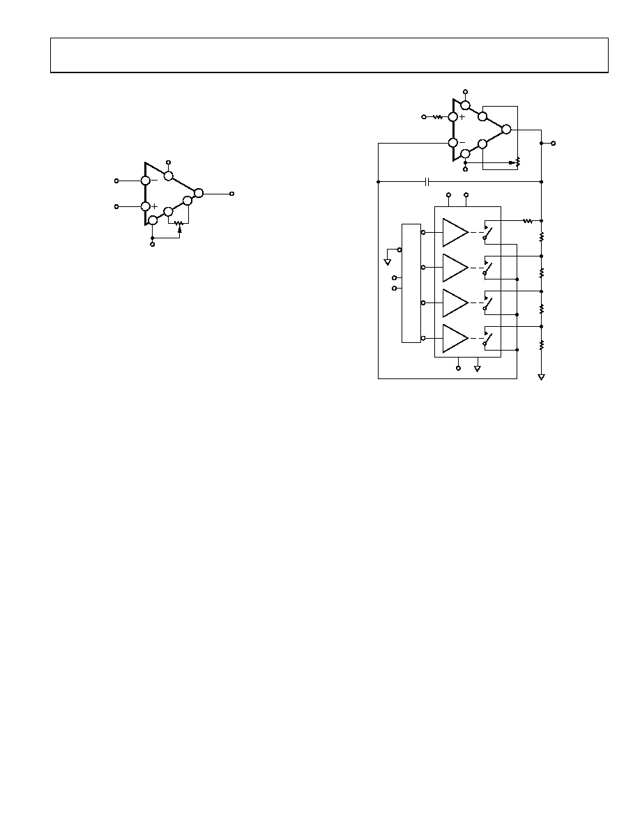
Input Offset Voltage Adjustment
Offset of AD8610 is very small and normally does not require
additional offset adjustment. However, the offset adjust pins can
be used as shown in Figure 66 to further reduce the dc offset. By
using resistors in the range of 50 kΩ, offset trim range is ±3.3 mV.
R1
V+
VOUT
V–
AD8610
02
73
0-
0
6
7
6
1
5
4
3
2
Figure 66. Offset Voltage Nulling Circuit
Programmable Gain Amplifier (PGA)
The combination of low noise, low input bias current, low input
offset voltage, and low temperature drift make the AD8610/
AD8620 a perfect solution for programmable gain amplifiers.
PGAs are often used immediately after sensors to increase the
dynamic range of the measurement circuit. Historically, the large
on resistance of switches (combined with the large IB currents
of amplifiers) created a large dc offset in PGAs. Recent and
improved monolithic switches and amplifiers completely remove
these problems. A PGA discrete circuit is shown in Figure 67.
In Figure 67, when the 10 pA bias current of the AD8610 is
dropped across the (<5 Ω) RON of the switch, it results in a
negligible offset error.
When high precision resistors are used, as in the circuit of
Figure 67, the error introduced by the PGA is within the
LSB requirement for a 16-bit system.
VIN
VOUT
AD8610
7
4
6
5
1
2
3
IN1
S1
D1
10k
1k
+5V
–5V
IN2
S2
D2
IN3
S3
D3
IN4
S4
D4
ADG452
3
2
14
15
11
10
6
7
VL
VDD
13
12
1
16
9
8
74HC139
VSS
4
GND
5
1k
100
11
5pF
G = +1
G = +10
G = +100
G = +1000
+5V
–5V
Y0
Y1
Y2
Y3
G
A
B
A0
A1
02
73
0
-06
7
100
Figure 67. High Precision PGA
1. Room temperature error calculation due to RON and IB
ΔVOS = IB × RON = 2 pA × 5 Ω = 10 pV
Total Offset = AD8610 (Offset) + ΔVOS
Total Offset = AD8610 (Offset_Trimmed) + ΔVOS
Total Offset = 5 μV + 10 pV ≈ 5 μV
2. Full temperature error calculation due to RON and IB
ΔVOS (@ 85°C) = IB (@ 85°C) × RON (@ 85°C) =
250 pA × 15 Ω = 3.75 nV
3. The temperature coefficient of switch and AD8610/AD8620
combined is essentially the same as the TCVOS of the
AD8610/AD8620.
ΔVOS/ΔT(total) = ΔVOS/ΔT(AD8610/AD8620) +
ΔVOS/ΔT(IB × RON)
ΔVOS/ΔT(total) = 0.5 μV/°C + 0.06 nV/°C ≈ 0.5 μV/°C
相关PDF资料 |
PDF描述 |
|---|---|
| 9208BLK | LUG SPADE .250" ISULATED BLACK |
| TV04A600JB-HF | TVS 400W 60V BIDIRECT 5% SMA |
| TV04A5V0JB-HF | TVS 400W 5V BIDIRECT 5% SMA |
| OP37EZ | IC OPAMP GP 63MHZ LN PREC 8DIP |
| TV04A580JB-HF | TVS 400W 58V BIDIRECT 5% SMA |
相关代理商/技术参数 |
参数描述 |
|---|---|
| AD8620BRZ-REEL7 | 功能描述:IC OPAMP JFET 25MHZ DUAL 8SOIC RoHS:是 类别:集成电路 (IC) >> Linear - Amplifiers - Instrumentation 系列:- 标准包装:2,500 系列:Excalibur™ 放大器类型:J-FET 电路数:1 输出类型:- 转换速率:45 V/µs 增益带宽积:10MHz -3db带宽:- 电流 - 输入偏压:20pA 电压 - 输入偏移:490µV 电流 - 电源:1.7mA 电流 - 输出 / 通道:48mA 电压 - 电源,单路/双路(±):4.5 V ~ 38 V,±2.25 V ~ 19 V 工作温度:-40°C ~ 85°C 安装类型:表面贴装 封装/外壳:8-SOIC(0.154",3.90mm 宽) 供应商设备封装:8-SOIC 包装:带卷 (TR) |
| AD8622 | 制造商:AD 制造商全称:Analog Devices 功能描述:Dual, Low Power, Low Noise, Low Bias Current Precision Rail-to-Rail Output Op Amp |
| AD8622_09 | 制造商:AD 制造商全称:Analog Devices 功能描述:Dual, Low Power, Precision Rail-to-Rail Output Op Amp |
| AD8622ARMZ | 功能描述:IC OPAMP GP R-R 540KHZ LP 8MSOP RoHS:是 类别:集成电路 (IC) >> Linear - Amplifiers - Instrumentation 系列:- 标准包装:2,500 系列:- 放大器类型:通用 电路数:4 输出类型:- 转换速率:0.6 V/µs 增益带宽积:1MHz -3db带宽:- 电流 - 输入偏压:45nA 电压 - 输入偏移:2000µV 电流 - 电源:1.4mA 电流 - 输出 / 通道:40mA 电压 - 电源,单路/双路(±):3 V ~ 32 V,±1.5 V ~ 16 V 工作温度:0°C ~ 70°C 安装类型:表面贴装 封装/外壳:14-TSSOP(0.173",4.40mm 宽) 供应商设备封装:14-TSSOP 包装:带卷 (TR) 其它名称:LM324ADTBR2G-NDLM324ADTBR2GOSTR |
| AD8622ARMZ | 制造商:Analog Devices 功能描述:OP-AMP, PRECISION, 560KHZ, 0.48V/us, MSO |
发布紧急采购,3分钟左右您将得到回复。