- 您现在的位置:买卖IC网 > PDF目录373958 > AD9054PCB (Analog Devices, Inc.) 8-Bit, 200 MSPS A/D Converter PDF资料下载
参数资料
| 型号: | AD9054PCB |
| 厂商: | Analog Devices, Inc. |
| 英文描述: | 8-Bit, 200 MSPS A/D Converter |
| 中文描述: | 8位,200 MSPS的A / D转换 |
| 文件页数: | 12/20页 |
| 文件大小: | 303K |
| 代理商: | AD9054PCB |
AD9054
–12–
REV. 0
When driven differentially, ENCODE and DS will accommo-
date differential signals centered between 1.5 V and 4.5 V with
a total differential swing
≥
800 mV (V
ID
≥
400 mV).
Note the 6-diode clock input protection circuitry in Figure 5.
T his limits the differential input voltage to ~
±
2.1 V. When the
diodes turn on, current is limited by the 300
series resistor.
Exceeding 2.1 V across the differential inputs will have no im-
pact on the performance of the converter, but be aware of the
clock signal distortion that may be produced by the nonlinear
impedance at the converter.
CLOCK
CLOCK
ENC
ENC
V
IH D
V
IC M
V
IL D
CLOCK
ENC
ENC
V
IH D
V
IC M
V
IL D
0.1
m
F
V
ID
V
ID
a. Driving Differential Inputs Differentially
b. Driving Differential Inputs Single-Endedly
Figure 34. Input Signal Level Definitions
Single Port Mode
When operated in a Single Port mode (
DEMUX
= HIGH), the
timing of the AD9054 is similar to any high speed A/D Con-
verter (Figure 1).
A sample is taken on every rising edge of ENCODE, and the
resulting data is produced on the output pins following the
FOURT H rising edge of ENCODE after the sample was taken
(four pipeline delays). T he output data are valid t
PD
after the
rising edge of ENCODE, and remain valid until at least t
V
after
the next rising edge of ENCODE.
T he maximum clock rate is specified as 100 MSPS. T his is
recommended because the guaranteed output data valid time
equals the Clock Period (1/f
S
) minus the Output Propagation
Delay (t
PD
) plus the Output Valid T ime (t
V
), which comes to
4.8 ns at 100 MHz. T his is about as fast as standard logic is able
to capture the data with reasonable design margins. T he AD9054
will operate faster in single-channel mode if you are able to
capture the data.
When operating in Single-Channel Mode, the outputs at Port B
are held static in a random state.
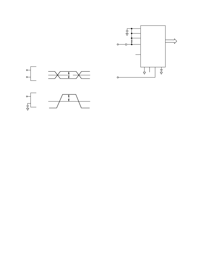
Figure 35 shows the AD9054 used in single-channel output
mode. T he analog input (
±
0.5 V) is ac coupled and the ENCODE
input is driven by a T T L level signal. T he chip’s internal refer-
ence is used.
VIN
0.1
m
F
+5V
1k
V
0.1
m
F
0.1
m
F
NC
CLOCK
VREF OUT
VREF IN
AIN
AIN
DEMUX
AD9054
DS
DS
ENC
ENC
A PORT
NC = NO CONNECT
Figure 35. Single Port Mode—AC-Coupled Input—Single-
Ended Encode
Dual Port Mode
In Dual Port Mode (
DEMUX
= LOW), the conversion results
are alternated between the two output ports (Figure 2). T his
limits the data output rate at either port to 1/2 the conversion
rate (ENCODE), and supports conversion at up to 200 MSPS
with T T L/CMOS compatible interfaces. Dual Channel Mode is
required for guaranteed operation above 100 MSPS, but may be
enabled at any specified conversion rate.
T he multiplexing is controlled internally via a clock divider,
which introduces a degree of ambiguity in the port assignments.
Figure 2 illustrates that, prior to synchronization, either Port A
or Port B may produce the even or odd samples. T his is re-
solved by exercising the Data Sync (DS) control, a differential
input (identical to the ENCODE input), which facilitates opera-
tion at high speed.
At least once after power-up, and prior to using the conversion
data, the part needs to be synchronized by a falling edge (or a
positive-going pulse) on DS (observing setup and hold times
with respect to ENCODE). If the converter’s internal timing is
in conflict with the DS signal when it is exercised, then two data
samples (one on each port) are corrupted as the converter is
resynchronized. T he converter then produces data with a
known phase relationship from that point forward.
Note that if the converter is already properly synchronized, the
DS pulse has no effect on the output data. T his allows the con-
verter to be continuously resynchronized by a pulse at 1/2 the
ENCODE rate. T his signal is often available within a system, as
it represents the master clock rate for the demultiplexed output
data. Of course, a single DS signal may be used to synchronize
multiple A/D converters in a multichannel system.
Applications that call for the AD9054 to be synchronized at
power-up or only periodically during calibration/reset (i.e., valid
data is not required prior to synchronization), need only be
concerned with the timing of the falling edge of DS. T he falling
edge of DS must satisfy the setup time defined by Figure 2 and
相关PDF资料 |
PDF描述 |
|---|---|
| AD9057 | 8-Bit 40 MSPS/60 MSPS/80 MSPS A/D Converter |
| AD9057BRS-80 | 8-Bit 40 MSPS/50 MSPS/80 MSPS Converter |
| AD9057BRS-40 | 8-Bit 40 MSPS/50 MSPS/80 MSPS Converter |
| AD9057BRS-60 | 8-Bit 40 MSPS/60 MSPS/80 MSPS A/D Converter |
| AD9057PCB | 8-Bit 40 MSPS/60 MSPS/80 MSPS A/D Converter |
相关代理商/技术参数 |
参数描述 |
|---|---|
| AD9057 | 制造商:AD 制造商全称:Analog Devices 功能描述:8-Bit 40 MSPS/60 MSPS/80 MSPS A/D Converter |
| AD9057/PCB | 制造商:Analog Devices 功能描述:EVAL KIT FOR ADC, 8BIT 40MSPS/60MSPS/80MSPS A/D CNVRTR - Bulk |
| AD9057_03 | 制造商:AD 制造商全称:Analog Devices 功能描述:8-Bit 40 MSPS/60 MSPS/80 MSPS A/D Converter |
| AD9057-40 | 制造商:AD 制造商全称:Analog Devices 功能描述:8-Bit 40 MSPS/60 MSPS/80 MSPS A/D Converter |
| AD9057-60 | 制造商:AD 制造商全称:Analog Devices 功能描述:8-Bit 40 MSPS/60 MSPS/80 MSPS A/D Converter |
发布紧急采购,3分钟左右您将得到回复。