- 您现在的位置:买卖IC网 > PDF目录17025 > AD9204-80EBZ (Analog Devices Inc)BOARD EVALUATION 80MSPS AD9204 PDF资料下载
参数资料
| 型号: | AD9204-80EBZ |
| 厂商: | Analog Devices Inc |
| 文件页数: | 22/36页 |
| 文件大小: | 0K |
| 描述: | BOARD EVALUATION 80MSPS AD9204 |
| 设计资源: | AD9650,92xx Schematic AD92xx/AD9650 Gerber Files |
| 标准包装: | 1 |
| ADC 的数量: | 2 |
| 位数: | 10 |
| 采样率(每秒): | 80M |
| 数据接口: | 串行,SPI? |
| 输入范围: | 1 ~ 2 Vpp |
| 在以下条件下的电源(标准): | 177mW @ 80MSPS |
| 工作温度: | -40°C ~ 85°C |
| 已用 IC / 零件: | AD9204 |
| 已供物品: | 板 |
第1页第2页第3页第4页第5页第6页第7页第8页第9页第10页第11页第12页第13页第14页第15页第16页第17页第18页第19页第20页第21页当前第22页第23页第24页第25页第26页第27页第28页第29页第30页第31页第32页第33页第34页第35页第36页
AD9204
Rev. 0 | Page 29 of 36
SERIAL PORT INTERFACE (SPI)
The AD9204 serial port interface (SPI) allows the user to configure
the converter for specific functions or operations through a
structured register space provided inside the ADC. The SPI
gives the user added flexibility and customization, depending
on the application. Addresses are accessed via the serial port
and can be written to or read from via the port. Memory is
organized into bytes that can be further divided into fields,
which are documented in the Memory Map section. For
detailed operational information, see the AN-877 Applica-
tion Note, Interfacing to High Speed ADCs via SPI.
CONFIGURATION USING THE SPI
Three pins define the SPI of this ADC: the SCLK, the SDIO,
and the CSB (see Table 14). The SCLK (a serial clock) is used
to synchronize the read and write data presented from and to
the ADC. The SDIO (serial data input/output) is a dual-purpose
pin that allows data to be sent and read from the internal ADC
memory map registers. The CSB (chip select bar) is an active-
low control that enables or disables the read and write cycles.
Table 14. Serial Port Interface Pins
Pin
Function
SCLK
Serial Clock. The serial shift clock input is used to
synchronize serial interface reads and writes.
SDIO
Serial Data Input/Output. A dual-purpose pin that
typically serves as an input or an output, depending
on the instruction being sent and the relative position
in the timing frame.
CSB
Chip Select Bar. An active-low control that gates the read
and write cycles.
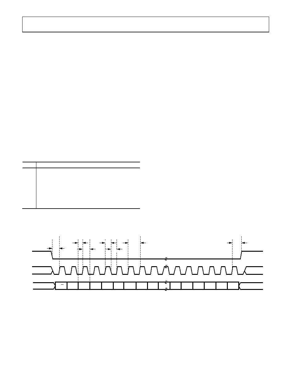
The falling edge of CSB, in conjunction with the rising edge of
SCLK, determines the start of the framing. An example of the
serial timing and its definitions can be found in Figure 58 and
Other modes involving the CSB are available. The CSB can be
held low indefinitely, which permanently enables the device;
this is called streaming. The CSB can stall high between bytes to
allow for additional external timing. When CSB is tied high, SPI
functions are placed in high impedance mode. This mode turns
on any SPI pin secondary functions.
During an instruction phase, a 16-bit instruction is transmitted.
Data follows the instruction phase, and its length is determined
by the W0 and W1 bits, as shown in Figure 58.
All data is composed of 8-bit words. The first bit of the first byte
in a multibyte serial data transfer frame indicates whether a read
command or a write command is issued. This allows the serial
data input/output (SDIO) pin to change direction from an input
to an output at the appropriate point in the serial frame.
In addition to word length, the instruction phase determines
whether the serial frame is a read or write operation, allowing
the serial port to be used both to program the chip and to read
the contents of the on-chip memory. If the instruction is a readback
operation, performing a readback causes the serial data input/
output (SDIO) pin to change direction from an input to an output
at the appropriate point in the serial frame.
Data can be sent in MSB-first mode or in LSB-first mode. MSB
first is the default on power-up and can be changed via the SPI
port configuration register. For more information about this
and other features, see the AN-877 Application Note, Interfacing
to High Speed ADCs via SPI.
DON’T CARE
SDIO
SCLK
CSB
tS
tDH
tCLK
tDS
tH
R/W
W1
W0
A12
A11
A10
A9
A8
A7
D5
D4
D3
D2
D1
D0
tLOW
tHIGH
0812
2-
023
Figure 58. Serial Port Interface Timing Diagram
相关PDF资料 |
PDF描述 |
|---|---|
| DK-V6-EMBD-G-J-XP1 | DEV KIT EMBEDDED VIRTEX 6 |
| 0982660813 | CBL 13POS 0.5MM JMPR TYPE A 2" |
| 0982660816 | CBL 13POS 0.5MM JMPR TYPE D 4" |
| DK-S6-EMBD-G-J-XP1 | DEV KIT EMBEDDED SPARTAN 6 |
| 0210490971 | CABLE JUMPER 1.25MM .102M 27POS |
相关代理商/技术参数 |
参数描述 |
|---|---|
| AD9204BCPZ-20 | 功能描述:IC ADC 10BIT 20MSPS DL 64LFCSP RoHS:是 类别:集成电路 (IC) >> 数据采集 - 模数转换器 系列:- 标准包装:1,000 系列:- 位数:12 采样率(每秒):300k 数据接口:并联 转换器数目:1 功率耗散(最大):75mW 电压电源:单电源 工作温度:0°C ~ 70°C 安装类型:表面贴装 封装/外壳:24-SOIC(0.295",7.50mm 宽) 供应商设备封装:24-SOIC 包装:带卷 (TR) 输入数目和类型:1 个单端,单极;1 个单端,双极 |
| AD9204BCPZ-40 | 功能描述:IC ADC 10BIT 40MSPS DL 64LFCSP RoHS:是 类别:集成电路 (IC) >> 数据采集 - 模数转换器 系列:- 标准包装:1 系列:microPOWER™ 位数:8 采样率(每秒):1M 数据接口:串行,SPI? 转换器数目:1 功率耗散(最大):- 电压电源:模拟和数字 工作温度:-40°C ~ 125°C 安装类型:表面贴装 封装/外壳:24-VFQFN 裸露焊盘 供应商设备封装:24-VQFN 裸露焊盘(4x4) 包装:Digi-Reel® 输入数目和类型:8 个单端,单极 产品目录页面:892 (CN2011-ZH PDF) 其它名称:296-25851-6 |
| AD9204BCPZ-65 | 功能描述:IC ADC 10BIT 65MSPS DL 64LFCSP RoHS:是 类别:集成电路 (IC) >> 数据采集 - 模数转换器 系列:- 其它有关文件:TSA1204 View All Specifications 标准包装:1 系列:- 位数:12 采样率(每秒):20M 数据接口:并联 转换器数目:2 功率耗散(最大):155mW 电压电源:模拟和数字 工作温度:-40°C ~ 85°C 安装类型:表面贴装 封装/外壳:48-TQFP 供应商设备封装:48-TQFP(7x7) 包装:Digi-Reel® 输入数目和类型:4 个单端,单极;2 个差分,单极 产品目录页面:1156 (CN2011-ZH PDF) 其它名称:497-5435-6 |
| AD9204BCPZ-80 | 功能描述:IC ADC 10BIT 80MSPS DL 64LFCSP RoHS:是 类别:集成电路 (IC) >> 数据采集 - 模数转换器 系列:- 标准包装:1 系列:microPOWER™ 位数:8 采样率(每秒):1M 数据接口:串行,SPI? 转换器数目:1 功率耗散(最大):- 电压电源:模拟和数字 工作温度:-40°C ~ 125°C 安装类型:表面贴装 封装/外壳:24-VFQFN 裸露焊盘 供应商设备封装:24-VQFN 裸露焊盘(4x4) 包装:Digi-Reel® 输入数目和类型:8 个单端,单极 产品目录页面:892 (CN2011-ZH PDF) 其它名称:296-25851-6 |
| AD9204BCPZRL7-20 | 功能描述:IC ADC 10BIT 20MSPS 64LFCSP RoHS:是 类别:集成电路 (IC) >> 数据采集 - 模数转换器 系列:- 标准包装:1,000 系列:- 位数:16 采样率(每秒):45k 数据接口:串行 转换器数目:2 功率耗散(最大):315mW 电压电源:模拟和数字 工作温度:0°C ~ 70°C 安装类型:表面贴装 封装/外壳:28-SOIC(0.295",7.50mm 宽) 供应商设备封装:28-SOIC W 包装:带卷 (TR) 输入数目和类型:2 个单端,单极 |
发布紧急采购,3分钟左右您将得到回复。