- 您现在的位置:买卖IC网 > PDF目录10215 > AD9214BRSZ-RL105 (Analog Devices Inc)IC ADC 10BIT 105MSPS 28-SSOP T/R PDF资料下载
参数资料
| 型号: | AD9214BRSZ-RL105 |
| 厂商: | Analog Devices Inc |
| 文件页数: | 17/20页 |
| 文件大小: | 0K |
| 描述: | IC ADC 10BIT 105MSPS 28-SSOP T/R |
| 标准包装: | 1,500 |
| 位数: | 10 |
| 采样率(每秒): | 105M |
| 数据接口: | 并联 |
| 转换器数目: | 1 |
| 功率耗散(最大): | 325mW |
| 电压电源: | 模拟和数字 |
| 工作温度: | -40°C ~ 85°C |
| 安装类型: | 表面贴装 |
| 封装/外壳: | 28-SSOP(0.209",5.30mm 宽) |
| 供应商设备封装: | 28-SSOP |
| 包装: | 带卷 (TR) |
| 输入数目和类型: | 2 个单端,单极;1 个差分,单极 |
REV. D
AD9214
–6–
PIN FUNCTION DESCRIPTIONS
Pin No.
Mnemonic
Function
1
OR
CMOS Output; Out-of-Range Indicator. Logic HIGH indicates the analog input voltage was
outside the converter’s range for the current output data.
2
DFS/GAIN
Data Format Select and Gain Mode Select. Connect externally to AVDD for two’s complement
data format and 1 V p-p analog input range. Connect externally to AGND for Offset Binary data
format and 1 V p-p analog input range. Connect externally to REF (Pin 4) for two’s complement
data format and 2 V p-p analog input range. Floating this pin will configure the device for Offset
Binary data format and a 2 V p-p analog input range.
3
REFSENSE
Reference Mode Select Pin for the ADC. This pin is normally connected externally to AGND,
which enables the internal 1.25 V reference, and configures REF (Pin 4) as an analog reference
output pin. Connecting REFSENSE externally to AVDD disables the internal reference, and config-
ures REF (Pin 4) as an external reference input. In this case, the user must drive REF with a clean
and accurate 1.25 V (
±5%) reference input.
4
REF
Reference input or output as configured by REFSENSE (Pin 3). When configured as an output
(REFSENSE = AGND), the internal reference (nominally 1.25 V) is enabled and is available to
the user on this pin. When configured as an input (REFSENSE = AVDD), the user must drive
REF with a clean and accurate 1.25 V (
±5%) reference. This pin should be bypassed to AGND
with an external 0.1
F capacitor, whether it is configured as an input or output.
5, 8, 11
AGND
Analog Ground
6, 7, 12
AVDD
Analog Power Supply, Nominally 3 V
9AIN
Positive terminal of the differential analog input for the ADC.
10
AIN
Negative terminal of the differential analog input for the ADC. This pin can be left open if
operating in single-ended mode, but it is preferable to match the impedance seen at the positive
terminal (see Driving the Analog Inputs).
13
ENCODE
Encode Clock for the ADC. The AD9214 samples the analog signal on the rising edge of ENCODE.
14
PWRDN
CMOS-compatible power-down mode select, Logic LOW for normal operation; Logic HIGH
for power-down mode (digital outputs in high impedance state). PWRDN has an internal
10 k
pull-down resistor to ground.
15, 23
DGND
Digital Output Ground
16, 24
DrVDD
Digital Output Driver Power Supply. Nominally 2.5 V to 3.6 V.
17–22, 25–28
D0 (LSB)–D5,
CMOS Digital Outputs of ADC
D6–D9 (MSB)
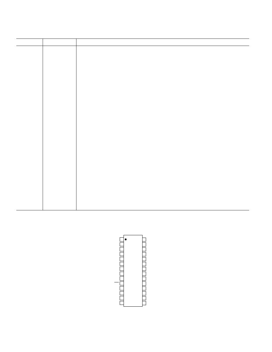
PIN CONFIGURATION
28-Lead Shrink Small Outline Package
TOP VIEW
(Not to Scale)
28
27
26
25
24
23
22
21
20
19
18
17
16
15
1
2
3
4
5
6
7
8
9
10
11
12
13
14
AD9214
PWRDN
ENCODE
AVDD
AGND
AIN
AGND
OR
DFS/GAIN
REFSENSE
REF
AVDD
AGND
DGND
DrVDD
D0 (LSB)
D1
D2
D3
D4
D9 (MSB)
D8
D7
D6
D5
DGND
DrVDD
相关PDF资料 |
PDF描述 |
|---|---|
| VI-2NK-IW-S | CONVERTER MOD DC/DC 40V 100W |
| VI-B2N-MW-F2 | CONVERTER MOD DC/DC 18.5V 100W |
| D38999/20MC98SN | CONN RCPT 10POS WALL MNT W/SCKT |
| AD7472ARU | IC ADC 12BIT PARALLEL 24-TSSOP |
| VI-B2N-MW-F1 | CONVERTER MOD DC/DC 18.5V 100W |
相关代理商/技术参数 |
参数描述 |
|---|---|
| AD9214BRSZ-RL65 | 功能描述:IC ADC 10BIT 65MSPS 28-SSOP T/R RoHS:是 类别:集成电路 (IC) >> 数据采集 - 模数转换器 系列:- 标准包装:1,000 系列:- 位数:16 采样率(每秒):45k 数据接口:串行 转换器数目:2 功率耗散(最大):315mW 电压电源:模拟和数字 工作温度:0°C ~ 70°C 安装类型:表面贴装 封装/外壳:28-SOIC(0.295",7.50mm 宽) 供应商设备封装:28-SOIC W 包装:带卷 (TR) 输入数目和类型:2 个单端,单极 |
| AD9214BRSZ-RL80 | 功能描述:IC ADC 10BIT 80MSPS 28-SSOP T/R RoHS:是 类别:集成电路 (IC) >> 数据采集 - 模数转换器 系列:- 标准包装:1,000 系列:- 位数:12 采样率(每秒):300k 数据接口:并联 转换器数目:1 功率耗散(最大):75mW 电压电源:单电源 工作温度:0°C ~ 70°C 安装类型:表面贴装 封装/外壳:24-SOIC(0.295",7.50mm 宽) 供应商设备封装:24-SOIC 包装:带卷 (TR) 输入数目和类型:1 个单端,单极;1 个单端,双极 |
| AD9215 | 制造商:Analog Devices 功能描述:- Bulk |
| AD9215_13 | 制造商:AD 制造商全称:Analog Devices 功能描述:10-Bit, 65/80/105 MSPS, 3 V A/D Converter |
| AD9215BCP-105 | 制造商:Analog Devices 功能描述:ADC Single Pipelined 105Msps 10-bit Parallel 32-Pin LFCSP EP 制造商:Analog Devices 功能描述:10BIT ADC 105MSPS 9215 LFCSP-32 |
发布紧急采购,3分钟左右您将得到回复。