- 您现在的位置:买卖IC网 > PDF目录373960 > AD9215BRU-80EB (Analog Devices, Inc.) Circular Connector; No. of Contacts:18; Series:D38999; Body Material:Metal; Connecting Termination:Crimp; Connector Shell Size:15; Circular Contact Gender:Pin; Circular Shell Style:Straight Plug; Insert Arrangement:15-18 PDF资料下载
参数资料
| 型号: | AD9215BRU-80EB |
| 厂商: | Analog Devices, Inc. |
| 元件分类: | 圆形连接器 |
| 英文描述: | Circular Connector; No. of Contacts:18; Series:D38999; Body Material:Metal; Connecting Termination:Crimp; Connector Shell Size:15; Circular Contact Gender:Pin; Circular Shell Style:Straight Plug; Insert Arrangement:15-18 |
| 中文描述: | 10位,65/80/105 MSPS的,3V的A / D转换 |
| 文件页数: | 16/36页 |
| 文件大小: | 1416K |
| 代理商: | AD9215BRU-80EB |
第1页第2页第3页第4页第5页第6页第7页第8页第9页第10页第11页第12页第13页第14页第15页当前第16页第17页第18页第19页第20页第21页第22页第23页第24页第25页第26页第27页第28页第29页第30页第31页第32页第33页第34页第35页第36页
AD9215
Table 7. Reference Configuration Summary
Selected Mode
Externally Supplied Reference AVDD
Internal 0.5 V Reference
Programmed Variable
Reference
Internally Programmed 1 V
Reference
Table 8. Digital Output Coding
Code VIN+ VIN Input Span =
2 V p-p (V)
1023
1.000
512
0
511
0.00195
0
1.00
Rev. A | Page 16 of 36
External SENSE
Connection
Internal Op Amp
Configuration
N/A
Voltage Follower (G = 1)
Noninverting (1 < G < 2)
Resulting VREF
(V)
N/A
0.5
0.5 × (1 +
R2
/
R1
)
Resulting Differential Span
(V p-p)
2 × External Reference
1.0
2 × VREF
VREF
External Divider
AGND to 0.2 V
Internal Divider
1.0
2.0
VIN+ VIN Input Span =
1 V p-p (V)
0.500
0
0.000978
0.5000
Digital Output Offset Binary
(D9D0)
11 1111 1111
10 0000 0000
01 1111 1111
00 0000 0000
Digital Output Twos
Complement (D9D0)
01 1111 1111
00 0000 0000
11 1111 1111
10 0000 0000
High speed, high resolution ADCs are sensitive to the quality
of the clock input. The degradation in SNR at a given full-scale
input frequency (f
INPUT
) due only to aperture jitter (t
A
) can be
calculated with the following equation
SNR Degradation
=
20 × log
10
[2 × π
×
f
INPUT
×
t
A
]
In the equation, the rms aperture jitter,
t
A
, represents the root-
sum square of all jitter sources, which include the clock input,
analog input signal, and ADC aperture jitter specification.
Undersampling applications are particularly sensitive to jitter.
The clock input should be treated as an analog signal in cases
where aperture jitter may affect the dynamic range of the
AD9215. Power supplies for clock drivers should be separated
from the ADC output driver supplies to avoid modulating the
clock signal with digital noise. Low jitter, crystal-controlled
oscillators make the best clock sources. If the clock is generated
from another type of source (by gating, dividing, or other meth-
ods), it should be retimed by the original clock at the last step.
Power Dissipation and Standby Mode
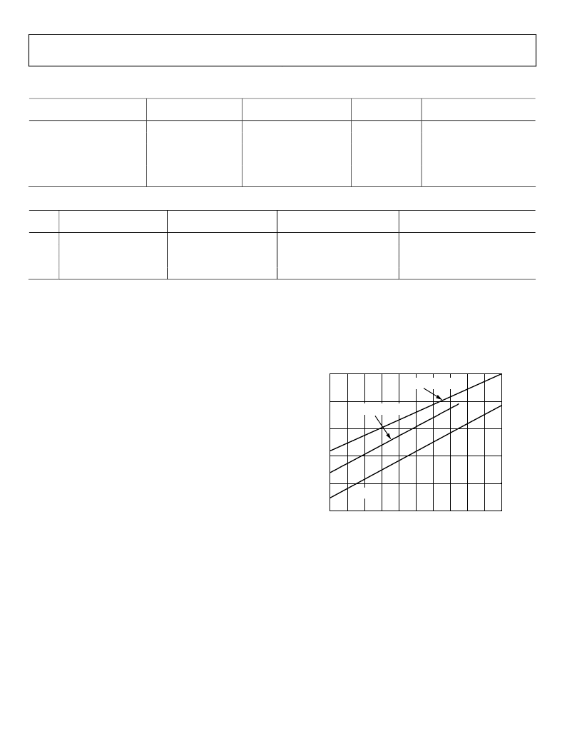
As shown in Figure 35, the power dissipated by the AD9215 is
proportional to its sample rate. The digital power dissipation
does not vary substantially between the three speed grades
because it is determined primarily by the strength of the digital
drivers and the load on each output bit. The maximum DRVDD
current can be calculated as
I
DRVDD
=
V
DRVDD
×
C
LOAD
×
f
CLOCK
×
N
where
N
is the number of output bits, 10 in the case of the
AD9215. This maximum current is for the condition of every
output bit switching on every clock cycle, which can only occur
for a full-scale square wave at the Nyquist frequency,
f
CLOCK
/2. In
practice, the DRVDD current is established by the average num-
ber of output bits switching, which are determined by the encode
rate and the characteristics of the analog input signal.
Digital power consumption can be minimized by reducing the
capacitive load presented to the output drivers. The data in
Figure 35 was taken with a 5 pF load on each output driver.
0
15
35
30
25
20
40
105
5
15
25
35
45
f
SAMPLE
(MSPS)
55
65
75
85
95
I
A
I
D
–1
1
3
5
7
9
11
13
15
AD9215-105 I
AVDD
AD9215-65/80 I
AVDD
I
DRVDD
Figure 35. Supply Current vs. f
SAMPLE
for f
IN
= 10.3 MHz
The analog circuitry is optimally biased so that each speed
grade provides excellent performance while affording reduced
power consumption. Each speed grade dissipates a baseline
power at low sample rates that increases linearly with the clock
frequency.
By asserting the PDWN pin high, the AD9215 is placed in
standby mode. In this state, the ADC typically dissipates 1 mW
if the CLK and analog inputs are static. During standby, the
output drivers are placed in a high impedance state. Reasserting
the PDWN pin low returns the AD9215 into its normal opera-
tional mode.
相关PDF资料 |
PDF描述 |
|---|---|
| AD9216BCPZRL7-65 | 10-Bit, 65/80/105 MSPS Dual A/D Converter |
| AD9216 | Static Monitor |
| AD9216-105 | 10-Bit, 65/80/105 MSPS Dual A/D Converter |
| AD9216-105PCB | 10-Bit, 65/80/105 MSPS Dual A/D Converter |
| AD9216-40PCB | 10-Bit, 65/80/105 MSPS Dual A/D Converter |
相关代理商/技术参数 |
参数描述 |
|---|---|
| AD9215BRURL7-105 | 制造商:AD 制造商全称:Analog Devices 功能描述:10-Bit, 65/80/105 MSPS, 3V A/D Converter |
| AD9215BRURL7-65 | 制造商:Rochester Electronics LLC 功能描述: 制造商:Analog Devices 功能描述: |
| AD9215BRURL7-80 | 制造商:Analog Devices 功能描述: |
| AD9215BRUZ-105 | 功能描述:IC ADC 10BIT 105MSPS 3V 28-TSSOP RoHS:是 类别:集成电路 (IC) >> 数据采集 - 模数转换器 系列:- 标准包装:1 系列:microPOWER™ 位数:8 采样率(每秒):1M 数据接口:串行,SPI? 转换器数目:1 功率耗散(最大):- 电压电源:模拟和数字 工作温度:-40°C ~ 125°C 安装类型:表面贴装 封装/外壳:24-VFQFN 裸露焊盘 供应商设备封装:24-VQFN 裸露焊盘(4x4) 包装:Digi-Reel® 输入数目和类型:8 个单端,单极 产品目录页面:892 (CN2011-ZH PDF) 其它名称:296-25851-6 |
| AD9215BRUZ-105 | 制造商:Analog Devices 功能描述:AD CONVERTOR ((NW)) |
发布紧急采购,3分钟左右您将得到回复。