- 您现在的位置:买卖IC网 > PDF目录10255 > AD9215BRUZ-65 (Analog Devices Inc)IC ADC 10BIT 65MSPS 3V 28TSSOP PDF资料下载
参数资料
| 型号: | AD9215BRUZ-65 |
| 厂商: | Analog Devices Inc |
| 文件页数: | 9/36页 |
| 文件大小: | 0K |
| 描述: | IC ADC 10BIT 65MSPS 3V 28TSSOP |
| 设计资源: | Very Low Jitter Encode (Sampling) Clocks for High Speed Analog-to-Digital Converters Using ADF4002 (CN0003) Interfacing the High Frequency AD8331 to AD9215 (CN0096) |
| 标准包装: | 50 |
| 位数: | 10 |
| 采样率(每秒): | 65M |
| 数据接口: | 并联 |
| 转换器数目: | 1 |
| 功率耗散(最大): | 96mW |
| 电压电源: | 单电源 |
| 工作温度: | -40°C ~ 85°C |
| 安装类型: | 表面贴装 |
| 封装/外壳: | 28-TSSOP(0.173",4.40mm 宽) |
| 供应商设备封装: | 28-TSSOP |
| 包装: | 管件 |
| 输入数目和类型: | 2 个单端,单极;1 个差分,单极 |
| 配用: | AD9215BCP-80EBZ-ND - BOARD EVAL FOR AD9215BCP-80 AD9215BCP-65EBZ-ND - BOARD EVAL FOR AD9215BCP-65 AD9215BCP-105EBZ-ND - BOARD EVAL FOR AD9215BCP-105 |
第1页第2页第3页第4页第5页第6页第7页第8页当前第9页第10页第11页第12页第13页第14页第15页第16页第17页第18页第19页第20页第21页第22页第23页第24页第25页第26页第27页第28页第29页第30页第31页第32页第33页第34页第35页第36页
Data Sheet
AD9215
Rev. B | Page 17 of 36
decoupling capacitors on REFT and REFB are discharged when
entering standby mode and then must be recharged when
returning to normal operation. As a result, the wake-up time is
related to the time spent in standby mode, and shorter standby
cycles result in proportionally shorter wake-up times. With the
recommended 0.1 μF and 10 μF decoupling capacitors on REFT
and REFB, it takes approximately one second to fully discharge
the reference buffer decoupling capacitors and 7 ms to restore
full operation.
Digital Outputs
The AD9215 output drivers can be configured to interface with
2.5 V or 3.3 V logic families by matching DRVDD to the digital
supply of the interfaced logic. The output drivers are sized to
provide sufficient output current to drive a wide variety of logic
families. However, large drive currents tend to cause current
glitches on the supplies that may affect converter performance.
Applications requiring the ADC to drive large capacitive loads
or large fanouts may require external buffers or latches.
Timing
The AD9215 provides latched data outputs with a pipeline delay
of five clock cycles. Data outputs are available one propagation
ure 2 for a detailed timing diagram.
The length of the output data lines and loads placed on them
should be minimized to reduce transients within the AD9215;
these transients can detract from the converter’s dynamic per-
formance.
The lowest typical conversion rate of the AD9215 is 5 MSPS. At
clock rates below 5 MSPS, dynamic performance may degrade.
Voltage Reference
A stable and accurate 0.5 V voltage reference is built into the
AD9215. The input range can be adjusted by varying the refer-
ence voltage applied to the AD9215, using either the internal
reference or an externally applied reference voltage. The input
span of the ADC tracks reference voltage changes linearly. Max-
imum SNR and DNL performance is achieved with the AD9215
set to the largest input span of 2 V p-p.
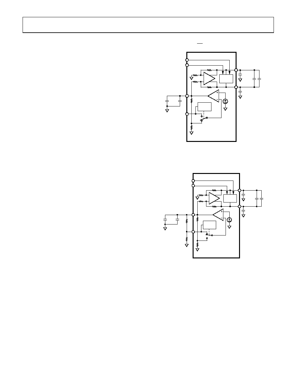
Internal Reference Connection
A comparator within the AD9215 detects the potential at the
SENSE pin and configures the reference into four possible
states, which are summarized in Table 1
. If SENSE is grounded,
the reference amplifier switch is connected to the internal resis-
tor divider (see Figure 36), setting VREF to 1 V. Connecting the
SENSE pin to the VREF pin switches the amplifier output to the
SENSE pin, configuring the internal op amp circuit as a voltage
follower and providing a 0.5 V reference output. If an external
resistor divider is connected as shown in Figure 37, the switch is
again set to the SENSE pin. This puts the reference amplifier in a
noninverting mode with the VREF output defined as
R1
R2
VREF
1
5
.
0
02874-A
-034
10
F
+
0.1
F
VREF
SENSE
0.5V
7k
7k
AD9215
VIN–
VIN+
REFT
0.1
F
0.1
F
10
F
0.1
F
REFB
SELECT
LOGIC
ADC
CORE
Figure 36. Internal Reference Configuration
In all reference configurations, REFT and REFB drive the ADC
conversion core and establish its input span. The input range of
the ADC always equals twice the voltage at the reference pin for
either an internal or an external reference.
02874-A-035
10
F
+
0.1
F
VREF
R2
R1
SENSE
0.5V
AD9215
VIN–
VIN+
REFT
0.1
F
0.1
F
10
F
0.1
F
REFB
SELECT
LOGIC
ADC
CORE
Figure 37. Programmable Reference Configuration
If the internal reference of the AD9215 is used to drive multiple
converters to improve gain matching, the loading of the refer-
ence by the other converters must be considered. Figure 38 de-
picts how the internal reference voltage is affected by loading.
相关PDF资料 |
PDF描述 |
|---|---|
| VI-23T-CU-F4 | CONVERTER MOD DC/DC 6.5V 200W |
| AD7858LARSZ-REEL | IC ADC 12BIT 8CHAN SRL 24SSOP |
| VI-23T-CU-F2 | CONVERTER MOD DC/DC 6.5V 200W |
| VE-22P-MX-F4 | CONVERTER MOD DC/DC 13.8V 75W |
| AD7858LARZ-REEL | IC ADC 12BIT 8CHAN SRL 24SOIC |
相关代理商/技术参数 |
参数描述 |
|---|---|
| AD9215BRUZ-65 | 制造商:Analog Devices 功能描述:10BIT ADC 65MSPS 9215 TSSOP28 |
| AD9215BRUZ-80 | 功能描述:IC ADC 10BIT 80MSPS 3V 28TSSOP RoHS:是 类别:集成电路 (IC) >> 数据采集 - 模数转换器 系列:- 其它有关文件:TSA1204 View All Specifications 标准包装:1 系列:- 位数:12 采样率(每秒):20M 数据接口:并联 转换器数目:2 功率耗散(最大):155mW 电压电源:模拟和数字 工作温度:-40°C ~ 85°C 安装类型:表面贴装 封装/外壳:48-TQFP 供应商设备封装:48-TQFP(7x7) 包装:Digi-Reel® 输入数目和类型:4 个单端,单极;2 个差分,单极 产品目录页面:1156 (CN2011-ZH PDF) 其它名称:497-5435-6 |
| AD9215BRUZ-80 | 制造商:Analog Devices 功能描述:10BIT ADC 80MSPS 9215 TSSOP28 |
| AD9215BRUZRL7-105 | 功能描述:IC ADC 10BIT 105MSPS 3V 28TSSOP RoHS:是 类别:集成电路 (IC) >> 数据采集 - 模数转换器 系列:- 标准包装:1,000 系列:- 位数:12 采样率(每秒):300k 数据接口:并联 转换器数目:1 功率耗散(最大):75mW 电压电源:单电源 工作温度:0°C ~ 70°C 安装类型:表面贴装 封装/外壳:24-SOIC(0.295",7.50mm 宽) 供应商设备封装:24-SOIC 包装:带卷 (TR) 输入数目和类型:1 个单端,单极;1 个单端,双极 |
| AD9215BRUZRL7-65 | 功能描述:IC ADC 10BIT 65MSPS 3V 28TSSOP RoHS:是 类别:集成电路 (IC) >> 数据采集 - 模数转换器 系列:- 标准包装:1,000 系列:- 位数:16 采样率(每秒):45k 数据接口:串行 转换器数目:2 功率耗散(最大):315mW 电压电源:模拟和数字 工作温度:0°C ~ 70°C 安装类型:表面贴装 封装/外壳:28-SOIC(0.295",7.50mm 宽) 供应商设备封装:28-SOIC W 包装:带卷 (TR) 输入数目和类型:2 个单端,单极 |
发布紧急采购,3分钟左右您将得到回复。