- 您现在的位置:买卖IC网 > PDF目录373960 > AD9218-65PCB (Analog Devices, Inc.) 10-Bit, 40/65/80/105 MSPS 3 V Dual A/D Converter PDF资料下载
参数资料
| 型号: | AD9218-65PCB |
| 厂商: | Analog Devices, Inc. |
| 英文描述: | 10-Bit, 40/65/80/105 MSPS 3 V Dual A/D Converter |
| 中文描述: | 10位,40/65/80/105 MSPS的3伏双A / D转换 |
| 文件页数: | 15/24页 |
| 文件大小: | 1591K |
| 代理商: | AD9218-65PCB |
REV. 0
AD9218
–15–
THEORY OF OPERATION
The AD9218 ADC architecture is a bit-per-stage pipeline-type
converter utilizing switch capacitor techniques. These stages
determine the 7 MSBs and drive a 3-bit flash. Each stage provides
sufficient overlap and error correction allowing optimization of
comparator accuracy. The input buffers are differential, and both
sets of inputs are internally biased. This allows the most flexible
use of ac-coupled or dc-coupled and differential or single-ended
input modes. The output staging block aligns the data, carries
out the error correction, and feeds the data to output buffers.
The set of output buffers are powered from a separate supply,
allowing adjustment of the output voltage swing. There is no
discernible difference in performance between the two channels.
USING THE AD9218
ENCODE Input
Any high-speed A/D converter is extremely sensitive to the
quality of the sampling clock provided by the user. A Track/
Hold circuit is essentially a mixer. Any noise, distortion, or
timing jitter on the clock will be combined with the desired
signal at the A/D output. For that reason, considerable care has
been taken in the design of the ENCODE input of the AD9218,
and the user is advised to give commensurate thought to the clock
source. The ENCODE input is fully TTL/CMOS-compatible.
Digital Outputs
The digital outputs are TTL/CMOS-compatible for lower
power consumption. During power-down, the output buffers
transition to a high impedance state. A data format selection
option supports either two
’
s complement (set high) or offset
binary output (set low) formats.
Analog Input
The analog input to the AD9218 is a differential buffer. For
best dynamic performance, impedance at AIN and
AIN
should
match. Special care was taken in the design of the analog input
section of the AD9218 to prevent damage and corruption of
data when the input is overdriven. The nominal input range is
1.024 V p-p. Optimum performance is obtained when the part is
driven differentially where common mode noise is minimized
and even order harmonics are reduced. An example of driving
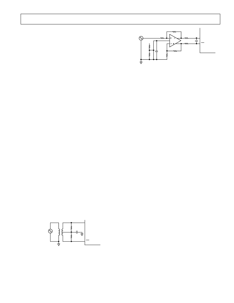
the AD9218 differentially via a wideband RF transformer for
ac-coupled applications is shown in Figure 12. Applications
that require dc-coupled differential drive can be accommo-
dated using the AD8138 differential output op amp, shown
in Figure 13.
25
25
0.1 F
1:1
A
IN
A
IN
AD9218
50
ANALOG
SIGNAL
SOURCE
Figure 12. Using a Wideband Transformer to Drive the
AD9218
10k
A
IN
A
IN
AD9218
50
ANALOG
SIGNAL
SOURCE
0.1 F
15pF
25
25
500
VOCM
500
500
525
5k
AV
DD
AD8138
Figure 13. Using the AD8138 to Drive the AD9218
Voltage Reference
A stable and accurate 1.25 V voltage reference is built into the
AD9218 (VREF OUT). In normal operation, the internal refer-
ence is used by strapping Pin 5 (REF
IN
A) and Pin 7 (REF
IN
B)
to Pin 6 (REF
OUT
). The input range for each channel can be
adjusted independently by varying the reference voltage inputs
applied to the AD9218. No appreciable degradation in per-
formance occurs when the reference is adjusted
±
5%. The
full-scale range of the ADC tracks reference voltage, which
changes linearly.
Timing
The AD9218 provides latched data outputs, with five pipeline
delays. Data outputs are available one propagation delay (t
PD
)
after the rising edge of the encode command (see Timing Dia-
gram). The length of the output data lines and loads placed
on them should be minimized to reduce transients within the
AD9218. These transients can detract from the converter
’
s
dynamic performance.
The minimum guaranteed conversion rate of the AD9218 is
20 MSPS. At clock rates below 20 MSPS, dynamic performance
will degrade.
User Select Options
Two pins are available for a combination of operational modes.
These options allow the user to power-down both channels,
excluding the reference, or just the B channel. Both modes place
the output buffers in a high impedance state. Recovery from a
power-down state is accomplished in 10 clock cycles following
power-on.
The other option allows the user to skew the B Channel output
data by one-half a clock cycle. In other words, if two clocks are
fed to the AD9218 and are 180 degrees out of phase, enabling
the data align will allow Channel B output data to be available
at the rising edge of Clock A. If the same encode clock is pro-
vided to both channels and the data align pin is enabled, output
data from Channel B will be 180 degrees out of phase with
respect to Channel A. If the same encode clock is provided to
both channels and the data align pin is disabled, both outputs are
delivered on the same rising edge of the clock.
相关PDF资料 |
PDF描述 |
|---|---|
| AD9218BST-40 | 10-Bit, 40/65/80/105 MSPS 3 V Dual A/D Converter |
| AD9218BST-65 | 10-Bit, 40/65/80/105 MSPS 3 V Dual A/D Converter |
| AD9220 | Complete 12-Bit 1.5/3.0/10.0 MSPS Monolithic A/D Converters |
| AD9223ARS | Complete 12-Bit 1.5/3.0/10.0 MSPS Monolithic A/D Converters |
| AD9220AR | Complete 12-Bit 1.5/3.0/10.0 MSPS Monolithic A/D Converters |
相关代理商/技术参数 |
参数描述 |
|---|---|
| AD9218BST-105 | 功能描述:IC ADC 10BIT DUAL 105MSPS 48LQFP RoHS:否 类别:集成电路 (IC) >> 数据采集 - 模数转换器 系列:- 标准包装:1 系列:- 位数:14 采样率(每秒):83k 数据接口:串行,并联 转换器数目:1 功率耗散(最大):95mW 电压电源:双 ± 工作温度:0°C ~ 70°C 安装类型:通孔 封装/外壳:28-DIP(0.600",15.24mm) 供应商设备封装:28-PDIP 包装:管件 输入数目和类型:1 个单端,双极 |
| AD9218BST-40 | 制造商:Analog Devices 功能描述:ADC Dual Pipelined 40Msps 10-bit Parallel 48-Pin LQFP 制造商:Rochester Electronics LLC 功能描述:DUAL 10 BIT 105/80/65/40 MSPS ADC - Bulk 制造商:Analog Devices 功能描述:SEMICONDUCTOR ((NW)) |
| AD9218BST-65 | 制造商:Analog Devices 功能描述:ADC Dual Pipelined 65Msps 10-bit Parallel 48-Pin LQFP 制造商:Rochester Electronics LLC 功能描述:DUAL 10 BIT 105/80/65 MSPS ADC - Bulk 制造商:Analog Devices 功能描述:IC 10-BIT ADC |
| AD9218BST-80 | 制造商:Analog Devices 功能描述:ADC Dual Pipelined 80Msps 10-bit Parallel 48-Pin LQFP 制造商:Analog Devices 功能描述:IC 10-BIT ADC |
| AD9218BST-RL105 | 功能描述:IC ADC 10BIT DUAL 105MSPS 48LQFP RoHS:否 类别:集成电路 (IC) >> 数据采集 - 模数转换器 系列:- 标准包装:1 系列:- 位数:14 采样率(每秒):83k 数据接口:串行,并联 转换器数目:1 功率耗散(最大):95mW 电压电源:双 ± 工作温度:0°C ~ 70°C 安装类型:通孔 封装/外壳:28-DIP(0.600",15.24mm) 供应商设备封装:28-PDIP 包装:管件 输入数目和类型:1 个单端,双极 |
发布紧急采购,3分钟左右您将得到回复。