- 您现在的位置:买卖IC网 > PDF目录17027 > AD9233-125EBZ (Analog Devices Inc)BOARD EVALUATION FOR AD9233 PDF资料下载
参数资料
| 型号: | AD9233-125EBZ |
| 厂商: | Analog Devices Inc |
| 文件页数: | 1/44页 |
| 文件大小: | 0K |
| 描述: | BOARD EVALUATION FOR AD9233 |
| 标准包装: | 1 |
| ADC 的数量: | 1 |
| 位数: | 12 |
| 采样率(每秒): | 125M |
| 数据接口: | 串行 |
| 输入范围: | 1 ~ 2 Vpp |
| 在以下条件下的电源(标准): | 455mW @125MSPS |
| 工作温度: | -40°C ~ 85°C |
| 已用 IC / 零件: | AD9233 |
| 已供物品: | 板,电源 |
| 相关产品: | AD9233BCPZRL7-125-ND - IC ADC 12BIT 125MSPS 48-LFCSP AD9233BCPZRL7-105-ND - IC ADC 12BIT 105MSPS 48-LFCSP AD9233BCPZ-105-ND - IC ADC 12BIT 105MSPS 48-LFCSP AD9233BCPZ-125-ND - IC ADC 12BIT 80/105/125 48-LFCSP AD9233BCPZ-80-ND - IC ADC 12BIT 80MSPS 48-LFCSP |
当前第1页第2页第3页第4页第5页第6页第7页第8页第9页第10页第11页第12页第13页第14页第15页第16页第17页第18页第19页第20页第21页第22页第23页第24页第25页第26页第27页第28页第29页第30页第31页第32页第33页第34页第35页第36页第37页第38页第39页第40页第41页第42页第43页第44页
12-Bit, 80 MSPS/105 MSPS/125 MSPS,
1.8 V Analog-to-Digital Converter
AD9233
Rev. A
Information furnished by Analog Devices is believed to be accurate and reliable. However, no
responsibilityis assumedbyAnalogDevicesforitsuse,norforanyinfringements of patents or other
rightsofthirdpartiesthatmayresultfromitsuse.Specificationssubjecttochangewithoutnotice.No
license is granted by implication or otherwise under any patent or patent rights of Analog Devices.
Trademarksandregisteredtrademarksarethepropertyoftheirrespectiveowners.
One Technology Way, P.O. Box 9106, Norwood, MA 02062-9106, U.S.A.
Tel: 781.329.4700
www.analog.com
Fax: 781.461.3113
2006 Analog Devices, Inc. All rights reserved.
FEATURES
1.8 V analog supply operation
1.8 V to 3.3 V output supply
SNR = 69.5 dBc (70.5 dBFS) to 70 MHz input
SFDR = 85 dBc to 70 MHz input
Low power: 395 mW @ 125 MSPS
Differential input with 650 MHz bandwidth
On-chip voltage reference and sample-and-hold amplifier
DNL = ±0.15 LSB
Flexible analog input: 1 V p-p to 2 V p-p range
Offset binary, Gray code, or twos complement data format
Clock duty cycle stabilizer
Data output clock
Serial port control
Built-in selectable digital test pattern generation
Programmable clock and data alignment
APPLICATIONS
Ultrasound equipment
IF sampling in communications receivers
IS-95, CDMA-One, IMT-2000
Battery-powered instruments
Hand-held scopemeters
Low cost digital oscilloscopes
GENERAL DESCRIPTION
The AD9233 is a monolithic, single 1.8 V supply, 12-bit, 80 MSPS/
105 MSPS/125 MSPS analog-to-digital converter (ADC), featuring
a high performance sample-and-hold amplifier (SHA) and on-
chip voltage reference. The product uses a multistage differential
pipeline architecture with output error correction logic to
provide 12-bit accuracy at 125 MSPS data rates and guarantees
no missing codes over the full operating temperature range.
The wide bandwidth, truly differential SHA allows a variety of
user-selectable input ranges and offsets, including single-ended
applications. It is suitable for multiplexed systems that switch
full-scale voltage levels in successive channels and for sampling
single-channel inputs at frequencies well beyond the Nyquist rate.
Combined with power and cost savings over previously available
ADCs, the AD9233 is suitable for applications in communications,
imaging, and medical ultrasound.
A differential clock input controls all internal conversion cycles. A
duty cycle stabilizer (DCS) compensates for wide variations in the
clock duty cycle while maintaining excellent overall ADC
performance.
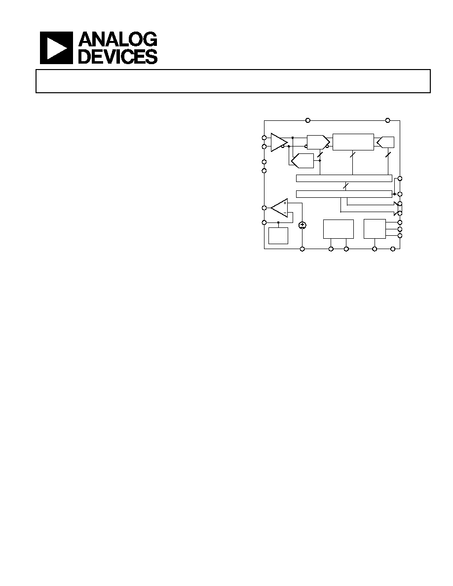
FUNCTIONAL BLOCK DIAGRAM
DRVDD
AVDD
AGND
0.5V
CLK–
PDWN DRGND
OR
VIN+
VIN–
REFT
REFB
AD9233
VREF
SENSE
SHA
A/D
MDAC1
4
8
13
3
A/D
8-STAGE
1 1/2-BIT PIPELINE
REF
SELECT
CLK+
CLOCK
DUTY CYCLE
STABILIZER
MODE
SELECT
CORRECTION LOGIC
OUTPUT BUFFERS
DCO
SCLK/DFS
SDIO/DCS
CSB
D11 (MSB)
D0 (LSB)
05492-
001
Figure 1.
The digital output data is presented in offset binary, Gray code, or
twos complement formats. A data output clock (DCO) is provided
to ensure proper latch timing with receiving logic.
The AD9233 is available in a 48-lead LFCSP and is specified
over the industrial temperature range (40°C to +85°C).
PRODUCT HIGHLIGHTS
1.
The AD9233 operates from a single 1.8 V power supply
and features a separate digital output driver supply to
accommodate 1.8 V to 3.3 V logic families.
2.
The patented SHA input maintains excellent performance
for input frequencies up to 225 MHz.
3.
The clock DCS maintains overall ADC performance over a
wide range of clock pulse widths.
4.
A standard serial port interface supports various product
features and functions, such as data formatting (offset
binary, twos complement, or Gray coding), enabling the
clock DCS, power-down, and voltage reference mode.
5.
The AD9233 is pin compatible with the AD9246, allowing
a simple migration from 12 bits to 14 bits.
相关PDF资料 |
PDF描述 |
|---|---|
| LGU2D681MELB | CAP ALUM 680UF 200V 20% SNAP |
| GCM22DRUN | CONN EDGECARD 44POS DIP .156 SLD |
| AD9204-20EBZ | BOARD EVALUATION 20MSPS AD9204 |
| GCM22DRUH | CONN EDGECARD 44POS DIP .156 SLD |
| AD9204-40EBZ | BOARD EVALUATION 40MSPS AD9204 |
相关代理商/技术参数 |
参数描述 |
|---|---|
| AD9233-80EB | 制造商:Analog Devices 功能描述: |
| AD9233-80EBZ | 功能描述:BOARD EVAL FOR AD9233 RoHS:是 类别:编程器,开发系统 >> 评估板 - 模数转换器 (ADC) 系列:- 产品培训模块:Obsolescence Mitigation Program 标准包装:1 系列:- ADC 的数量:1 位数:12 采样率(每秒):94.4k 数据接口:USB 输入范围:±VREF/2 在以下条件下的电源(标准):- 工作温度:-40°C ~ 85°C 已用 IC / 零件:MAX11645 已供物品:板,软件 |
| AD9233BCPZ-105 | 功能描述:IC ADC 12BIT 105MSPS 48-LFCSP RoHS:是 类别:集成电路 (IC) >> 数据采集 - 模数转换器 系列:- 其它有关文件:TSA1204 View All Specifications 标准包装:1 系列:- 位数:12 采样率(每秒):20M 数据接口:并联 转换器数目:2 功率耗散(最大):155mW 电压电源:模拟和数字 工作温度:-40°C ~ 85°C 安装类型:表面贴装 封装/外壳:48-TQFP 供应商设备封装:48-TQFP(7x7) 包装:Digi-Reel® 输入数目和类型:4 个单端,单极;2 个差分,单极 产品目录页面:1156 (CN2011-ZH PDF) 其它名称:497-5435-6 |
| AD9233BCPZ-125 | 功能描述:IC ADC 12BIT 80/105/125 48-LFCSP RoHS:是 类别:集成电路 (IC) >> 数据采集 - 模数转换器 系列:- 标准包装:1 系列:microPOWER™ 位数:8 采样率(每秒):1M 数据接口:串行,SPI? 转换器数目:1 功率耗散(最大):- 电压电源:模拟和数字 工作温度:-40°C ~ 125°C 安装类型:表面贴装 封装/外壳:24-VFQFN 裸露焊盘 供应商设备封装:24-VQFN 裸露焊盘(4x4) 包装:Digi-Reel® 输入数目和类型:8 个单端,单极 产品目录页面:892 (CN2011-ZH PDF) 其它名称:296-25851-6 |
| AD9233BCPZ-80 | 功能描述:IC ADC 12BIT 80MSPS 48-LFCSP RoHS:是 类别:集成电路 (IC) >> 数据采集 - 模数转换器 系列:- 其它有关文件:TSA1204 View All Specifications 标准包装:1 系列:- 位数:12 采样率(每秒):20M 数据接口:并联 转换器数目:2 功率耗散(最大):155mW 电压电源:模拟和数字 工作温度:-40°C ~ 85°C 安装类型:表面贴装 封装/外壳:48-TQFP 供应商设备封装:48-TQFP(7x7) 包装:Digi-Reel® 输入数目和类型:4 个单端,单极;2 个差分,单极 产品目录页面:1156 (CN2011-ZH PDF) 其它名称:497-5435-6 |
发布紧急采购,3分钟左右您将得到回复。