- 您现在的位置:买卖IC网 > PDF目录17024 > AD9233-80EBZ (Analog Devices Inc)BOARD EVAL FOR AD9233 PDF资料下载
参数资料
| 型号: | AD9233-80EBZ |
| 厂商: | Analog Devices Inc |
| 文件页数: | 10/44页 |
| 文件大小: | 0K |
| 描述: | BOARD EVAL FOR AD9233 |
| 标准包装: | 1 |
| ADC 的数量: | 1 |
| 位数: | 12 |
| 采样率(每秒): | 80M |
| 数据接口: | 串行,SPI? |
| 输入范围: | 1 ~ 2 Vpp |
| 在以下条件下的电源(标准): | 288mW @ 80kSPS |
| 工作温度: | -40°C ~ 85°C |
| 已用 IC / 零件: | AD9233 |
| 已供物品: | 板 |
第1页第2页第3页第4页第5页第6页第7页第8页第9页当前第10页第11页第12页第13页第14页第15页第16页第17页第18页第19页第20页第21页第22页第23页第24页第25页第26页第27页第28页第29页第30页第31页第32页第33页第34页第35页第36页第37页第38页第39页第40页第41页第42页第43页第44页
AD9233
Rev. A | Page 18 of 44
Table 9. Reference Configuration Summary
Selected Mode
SENSE Voltage
Resulting VREF (V)
Resulting Differential Span (V p-p)
External Reference
AVDD
N/A
2 × External Reference
Internal Fixed Reference
VREF
0.5
1.0
Programmable Reference
0.2 V to VREF
0.5 × (1 + R2/R1) (See Figure 43)
2 × VREF
Internal Fixed Reference
AGND to 0.2 V
1.0
2.0
0
–1.25
02
LOAD CURRENT (mA)
RE
F
E
RE
NCE
V
O
L
T
AG
E
RR
O
R
(
%
)
.0
–0.25
–0.50
–0.75
–1.00
0.5
1.0
1.5
VREF = 0.5V
VREF = 1V
0
549
2-
0
32
Figure 44. VREF Accuracy vs. Load
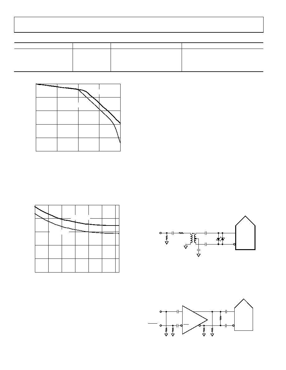
External Reference Operation
The use of an external reference may be necessary to enhance
the gain accuracy of the ADC or improve thermal drift
characteristics. Figure 45 shows the typical drift characteristics
of the internal reference in both 1 V and 0.5 V modes.
–40
–20
10
0
TEMPERATURE (°C)
RE
F
E
RE
NC
E
V
O
L
T
AG
E
RRO
R
(
m
V
)
8
6
4
2
80
0
204060
VREF = 0.5V
VREF = 1V
05
49
2-
0
33
Figure 45. Typical VREF Drift
When the SENSE pin is tied to the AVDD pin, the internal
reference is disabled, allowing the use of an external reference.
An internal resistor divider loads the external reference with an
equivalent 6 kΩ load (see Figure 11). In addition, an internal
buffer generates the positive and negative full-scale references
for the ADC core. Therefore, the external reference must be
limited to a maximum of 1 V.
CLOCK INPUT CONSIDERATIONS
For optimum performance, the AD9233 sample clock inputs
(CLK+ and CLK) should be clocked with a differential signal.
The signal is typically ac-coupled into the CLK+ pin and the
CLK pin via a transformer or capacitors. These pins are biased
internally (see Figure 5) and require no external bias.
Clock Input Options
The AD9233 has a very flexible clock input structure. The clock
input can be a CMOS, LVDS, LVPECL, or sine wave signal.
Regardless of the type of signal used, the jitter of the clock
source is of the most concern, as described in the Jitter
Considerations section.
Figure 46 shows one preferred method for clocking the
AD9233. A low jitter clock source is converted from single-
ended to a differential signal using an RF transformer. The
back-to-back Schottky diodes across the transformer secondary
limit clock excursions into the AD9233 to approximately
0.8 V p-p differential. This helps prevent the large voltage
swings of the clock from feeding through to other portions of
the AD9233 while preserving the fast rise and fall times of the
signal, which are critical to a low jitter performance.
05
49
2-
0
48
0.1F
SCHOTTKY
DIODES:
HSMS2812
CLOCK
INPUT
50
100
CLK–
CLK+
ADC
AD9233
MIN-CIRCUITS
ADT1–1WT, 1:1Z
XFMR
Figure 46. Transformer Coupled Differential Clock
If a low jitter clock source is not available, another option is to
ac-couple a differential PECL signal to the sample clock input
excellent jitter performance.
CLOCK
INPUT
100
0.1F
240
CLOCK
INPUT
054
92-
049
PECL DRIVER
50*
50*
CLK
*50 RESISTORS ARE OPTIONAL
CLK–
CLK+
ADC
AD9233
AD951x
Figure 47. Differential PECL Sample Clock
相关PDF资料 |
PDF描述 |
|---|---|
| LGU2D221MELY | CAP ALUM 220UF 200V 20% SNAP |
| STD21W-J | WIRE & CABLE MARKERS |
| AD962711-105EBZ | BOARD EVALUATION AD9627 105MSPS |
| UPB2D561MRD | CAP ALUM 560UF 200V 20% RADIAL |
| AD9609-80EBZ | BOARD EVALUATION AD9609 80MSPS |
相关代理商/技术参数 |
参数描述 |
|---|---|
| AD9233BCPZ-105 | 功能描述:IC ADC 12BIT 105MSPS 48-LFCSP RoHS:是 类别:集成电路 (IC) >> 数据采集 - 模数转换器 系列:- 其它有关文件:TSA1204 View All Specifications 标准包装:1 系列:- 位数:12 采样率(每秒):20M 数据接口:并联 转换器数目:2 功率耗散(最大):155mW 电压电源:模拟和数字 工作温度:-40°C ~ 85°C 安装类型:表面贴装 封装/外壳:48-TQFP 供应商设备封装:48-TQFP(7x7) 包装:Digi-Reel® 输入数目和类型:4 个单端,单极;2 个差分,单极 产品目录页面:1156 (CN2011-ZH PDF) 其它名称:497-5435-6 |
| AD9233BCPZ-125 | 功能描述:IC ADC 12BIT 80/105/125 48-LFCSP RoHS:是 类别:集成电路 (IC) >> 数据采集 - 模数转换器 系列:- 标准包装:1 系列:microPOWER™ 位数:8 采样率(每秒):1M 数据接口:串行,SPI? 转换器数目:1 功率耗散(最大):- 电压电源:模拟和数字 工作温度:-40°C ~ 125°C 安装类型:表面贴装 封装/外壳:24-VFQFN 裸露焊盘 供应商设备封装:24-VQFN 裸露焊盘(4x4) 包装:Digi-Reel® 输入数目和类型:8 个单端,单极 产品目录页面:892 (CN2011-ZH PDF) 其它名称:296-25851-6 |
| AD9233BCPZ-80 | 功能描述:IC ADC 12BIT 80MSPS 48-LFCSP RoHS:是 类别:集成电路 (IC) >> 数据采集 - 模数转换器 系列:- 其它有关文件:TSA1204 View All Specifications 标准包装:1 系列:- 位数:12 采样率(每秒):20M 数据接口:并联 转换器数目:2 功率耗散(最大):155mW 电压电源:模拟和数字 工作温度:-40°C ~ 85°C 安装类型:表面贴装 封装/外壳:48-TQFP 供应商设备封装:48-TQFP(7x7) 包装:Digi-Reel® 输入数目和类型:4 个单端,单极;2 个差分,单极 产品目录页面:1156 (CN2011-ZH PDF) 其它名称:497-5435-6 |
| AD9233BCPZRL7-105 | 功能描述:IC ADC 12BIT 105MSPS 48-LFCSP RoHS:是 类别:集成电路 (IC) >> 数据采集 - 模数转换器 系列:- 标准包装:1 系列:- 位数:14 采样率(每秒):83k 数据接口:串行,并联 转换器数目:1 功率耗散(最大):95mW 电压电源:双 ± 工作温度:0°C ~ 70°C 安装类型:通孔 封装/外壳:28-DIP(0.600",15.24mm) 供应商设备封装:28-PDIP 包装:管件 输入数目和类型:1 个单端,双极 |
| AD9233BCPZRL7-125 | 功能描述:IC ADC 12BIT 125MSPS 48-LFCSP RoHS:是 类别:集成电路 (IC) >> 数据采集 - 模数转换器 系列:- 标准包装:1 系列:- 位数:14 采样率(每秒):83k 数据接口:串行,并联 转换器数目:1 功率耗散(最大):95mW 电压电源:双 ± 工作温度:0°C ~ 70°C 安装类型:通孔 封装/外壳:28-DIP(0.600",15.24mm) 供应商设备封装:28-PDIP 包装:管件 输入数目和类型:1 个单端,双极 |
发布紧急采购,3分钟左右您将得到回复。