- 您现在的位置:买卖IC网 > PDF目录1986 > AD9237BCPZ-20 (Analog Devices Inc)IC ADC 12BIT SGL 20MSPS 32LFCSP PDF资料下载
参数资料
| 型号: | AD9237BCPZ-20 |
| 厂商: | Analog Devices Inc |
| 文件页数: | 8/24页 |
| 文件大小: | 0K |
| 描述: | IC ADC 12BIT SGL 20MSPS 32LFCSP |
| 产品变化通告: | Product Discontinuance 27/Oct/2011 |
| 标准包装: | 1 |
| 位数: | 12 |
| 采样率(每秒): | 20M |
| 数据接口: | 并联 |
| 转换器数目: | 3 |
| 功率耗散(最大): | 85mW |
| 电压电源: | 单电源 |
| 工作温度: | -40°C ~ 85°C |
| 安装类型: | 表面贴装 |
| 封装/外壳: | 32-VFQFN 裸露焊盘,CSP |
| 供应商设备封装: | 32-LFCSP-VQ(5x5) |
| 包装: | 托盘 |
| 输入数目和类型: | 2 个单端,单极;1 个差分,单极 |
AD9237
Data Sheet
Rev. B | Page 16 of 24
APPLYING THE AD9237
THEORY OF OPERATION
The AD9237 uses a calibrated, 11-stage pipeline architecture
with a patented input SHA implemented. Each stage of the
pipeline, excluding the last, consists of a low resolution flash
ADC connected to a switched capacitor digital-to-analog
converter (DAC) and an interstage residue amplifier (MDAC).
The MDAC magnifies the difference between the reconstructed
DAC output and the flash input for the next stage in the
pipeline. One bit of redundancy is used in each stage to facilitate
digital correction of flash errors. The last stage consists of a
flash ADC.
The pipelined architecture permits the first stage to operate on a
new input sample, while the remaining stages operate on preceding
samples. While the converter captures a new input sample every
clock cycle, it takes eight clock cycles for the conversion to be
fully processed and to appear at the output, as shown in Figure 2.
The input stage contains a differential SHA that can be ac- or
dc-coupled in differential or single-ended modes. The output-
staging block aligns the data, carries out the error correction,
and passes the data to the output buffers. The output buffers
are powered from a separate supply, allowing adjustment of
the output voltage swing. During power-down and stand-by
operation, the output buffers go into a high impedance state.
The ADC samples the analog input on the rising edge of
the clock. System disturbances just prior to, or immediately
following, the rising edge of the clock and/or excessive clock
jitter can cause the SHA to acquire the wrong input value and
should be minimized.
ANALOG INPUT AND REFERENCE OVERVIEW
The analog input to the AD9237 is a differential switched
capacitor SHA that has been designed for optimum
performance while processing a differential input signal.
The SHA input can support a wide common-mode range
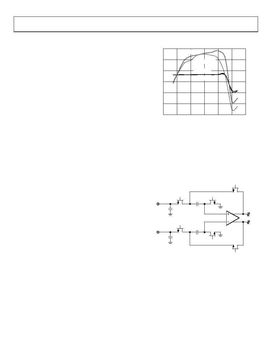
and maintain excellent performance, as shown in Figure 34.
An input common-mode voltage of midsupply minimizes
signal-dependant errors and provides optimum performance.
Figure 35 shows the clock signal alternately switching the
SHA between sample mode and hold mode. When the SHA is
switched into sample mode, the signal source must be capable
of charging the sample capacitors and settling within one-half
of a clock cycle. A small resistor in series with each input can
help reduce the peak transient current required from the output
stage of the driving source.
INPUT COMMON-MODE LEVEL (V)
S
NR/S
F
DR
(dBc
)
90
80
70
60
50
40
30
0
3.0
2.5
2.0
1.5
1.0
0.5
05455-038
2.5MHz SFDR
34.2MHz SFDR
2.5MHz SNR
34.2MHz SNR
Figure 34. AD9237-65 SNR/SFDR vs. Input Common-Mode Level
In addition, a small shunt capacitor placed across the inputs
provides dynamic charging currents. This passive network
creates a low-pass filter at the ADC’s input; therefore, the
precise values are dependent on the application. In IF under-
sampling applications, the shunt capacitor(s) should be reduced
or removed depending on the input frequency. In combination
with the driving source impedance, the capacitors limit the
input bandwidth.
05455-
039
VIN+
VIN–
CPAR
5pF
T
H
T
H
Figure 35. Switched-Capacitor SHA Input
For best dynamic performance, the source impedances driving
VIN+ and VIN– should be matched so that common-mode
settling errors are symmetrical. These errors are reduced by the
common-mode rejection of the ADC.
An internal differential reference buffer creates positive and
negative reference voltages, REFT and REFB, that define the
span of the ADC core.
相关PDF资料 |
PDF描述 |
|---|---|
| AD9238BSTRL-65 | IC ADC 12BIT DUAL 65MSPS 64-LQFP |
| AD9239BCPZ-170 | IC ADC 12BIT DUAL 170MSPS 72PIN |
| AD9240AS | IC ADC 14BIT 10MSPS 44-MQFP |
| AD9241ASZRL | IC ADC 14BIT SGL 1.25MSPS 44MQFP |
| AD9243ASZRL | IC ADC 14BIT SGL 3MSPS 44MQFP |
相关代理商/技术参数 |
参数描述 |
|---|---|
| AD9237BCPZ-40 | 功能描述:IC ADC 12BIT SGL 40MSPS 32LFCSP RoHS:是 类别:集成电路 (IC) >> 数据采集 - 模数转换器 系列:- 其它有关文件:TSA1204 View All Specifications 标准包装:1 系列:- 位数:12 采样率(每秒):20M 数据接口:并联 转换器数目:2 功率耗散(最大):155mW 电压电源:模拟和数字 工作温度:-40°C ~ 85°C 安装类型:表面贴装 封装/外壳:48-TQFP 供应商设备封装:48-TQFP(7x7) 包装:Digi-Reel® 输入数目和类型:4 个单端,单极;2 个差分,单极 产品目录页面:1156 (CN2011-ZH PDF) 其它名称:497-5435-6 |
| AD9237BCPZ-65 | 功能描述:IC ADC 12BIT SGL 65MSPS 32LFCSP RoHS:是 类别:集成电路 (IC) >> 数据采集 - 模数转换器 系列:- 产品培训模块:Lead (SnPb) Finish for COTS Obsolescence Mitigation Program 标准包装:2,500 系列:- 位数:12 采样率(每秒):3M 数据接口:- 转换器数目:- 功率耗散(最大):- 电压电源:- 工作温度:- 安装类型:表面贴装 封装/外壳:SOT-23-6 供应商设备封装:SOT-23-6 包装:带卷 (TR) 输入数目和类型:- |
| AD9237BCPZRL7-20 | 功能描述:IC ADC 12BIT SGL 20MSPS 32LFCSP RoHS:是 类别:集成电路 (IC) >> 数据采集 - 模数转换器 系列:- 产品培训模块:Lead (SnPb) Finish for COTS Obsolescence Mitigation Program 标准包装:2,500 系列:- 位数:12 采样率(每秒):3M 数据接口:- 转换器数目:- 功率耗散(最大):- 电压电源:- 工作温度:- 安装类型:表面贴装 封装/外壳:SOT-23-6 供应商设备封装:SOT-23-6 包装:带卷 (TR) 输入数目和类型:- |
| AD9237BCPZRL7-40 | 功能描述:IC ADC 12BIT SGL 40MSPS 32LFCSP RoHS:是 类别:集成电路 (IC) >> 数据采集 - 模数转换器 系列:- 标准包装:1,000 系列:- 位数:12 采样率(每秒):300k 数据接口:并联 转换器数目:1 功率耗散(最大):75mW 电压电源:单电源 工作温度:0°C ~ 70°C 安装类型:表面贴装 封装/外壳:24-SOIC(0.295",7.50mm 宽) 供应商设备封装:24-SOIC 包装:带卷 (TR) 输入数目和类型:1 个单端,单极;1 个单端,双极 |
| AD9237BCPZRL7-65 | 功能描述:IC ADC 12BIT SGL 65MSPS 32LFCSP RoHS:是 类别:集成电路 (IC) >> 数据采集 - 模数转换器 系列:- 产品培训模块:Lead (SnPb) Finish for COTS Obsolescence Mitigation Program 标准包装:2,500 系列:- 位数:12 采样率(每秒):3M 数据接口:- 转换器数目:- 功率耗散(最大):- 电压电源:- 工作温度:- 安装类型:表面贴装 封装/外壳:SOT-23-6 供应商设备封装:SOT-23-6 包装:带卷 (TR) 输入数目和类型:- |
发布紧急采购,3分钟左右您将得到回复。