- 您现在的位置:买卖IC网 > PDF目录10139 > AD9244BSTZRL-40 (Analog Devices Inc)IC ADC 14BIT SGL 40MSPS 48LQFP PDF资料下载
参数资料
| 型号: | AD9244BSTZRL-40 |
| 厂商: | Analog Devices Inc |
| 文件页数: | 10/36页 |
| 文件大小: | 0K |
| 描述: | IC ADC 14BIT SGL 40MSPS 48LQFP |
| 标准包装: | 2,000 |
| 位数: | 14 |
| 采样率(每秒): | 40M |
| 数据接口: | 并联 |
| 转换器数目: | 1 |
| 功率耗散(最大): | 300mW |
| 电压电源: | 模拟和数字 |
| 工作温度: | -40°C ~ 85°C |
| 安装类型: | 表面贴装 |
| 封装/外壳: | 48-LQFP |
| 供应商设备封装: | 48-LQFP(7x7) |
| 包装: | 带卷 (TR) |
| 输入数目和类型: | 2 个单端,单极;1 个差分,单极 |
第1页第2页第3页第4页第5页第6页第7页第8页第9页当前第10页第11页第12页第13页第14页第15页第16页第17页第18页第19页第20页第21页第22页第23页第24页第25页第26页第27页第28页第29页第30页第31页第32页第33页第34页第35页第36页
AD9244
Rev. C | Page 18 of 36
A differential input structure allows the user to easily configure the
inputs for either single-ended or differential operation. The ADC’s
input structure allows the dc offset of the input signal to be varied
independent of the input span of the converter. Specifically, the
input to the ADC core can be defined as the difference of the
voltages applied at the VIN+ and VIN– input pins.
Therefore, the equation
VCORE = (VIN+) – (VIN)
(1)
defines the output of the differential input stage and provides
the input to the ADC core. The voltage, VCORE, must satisfy the
condition
VREF/2 < VCORE < VREF/2
(2)
where VREF is the voltage at the VREF pin.
In addition to the limitations placed on the input voltages VIN+
and VIN– by Equation 1 and Equation 2, boundaries on the
inputs also exist based on the power supply voltages according
to the conditions
AGND 0.3 V < VIN+ < AVDD + 0.3 V
(3)
AGND 0.3 V < VIN < AVDD + 0.3 V
(4)
where:
AGND is nominally 0 V.
AVDD is nominally 5 V.
The range of valid inputs for VIN+ and VIN is any combination
that satisfies Equation 2, Equation 3, and Equation 4.
For additional information showing the relationship between
VIN+, VIN–, VREF, and the analog input range of the AD9244,
ANALOG INPUT OPERATION
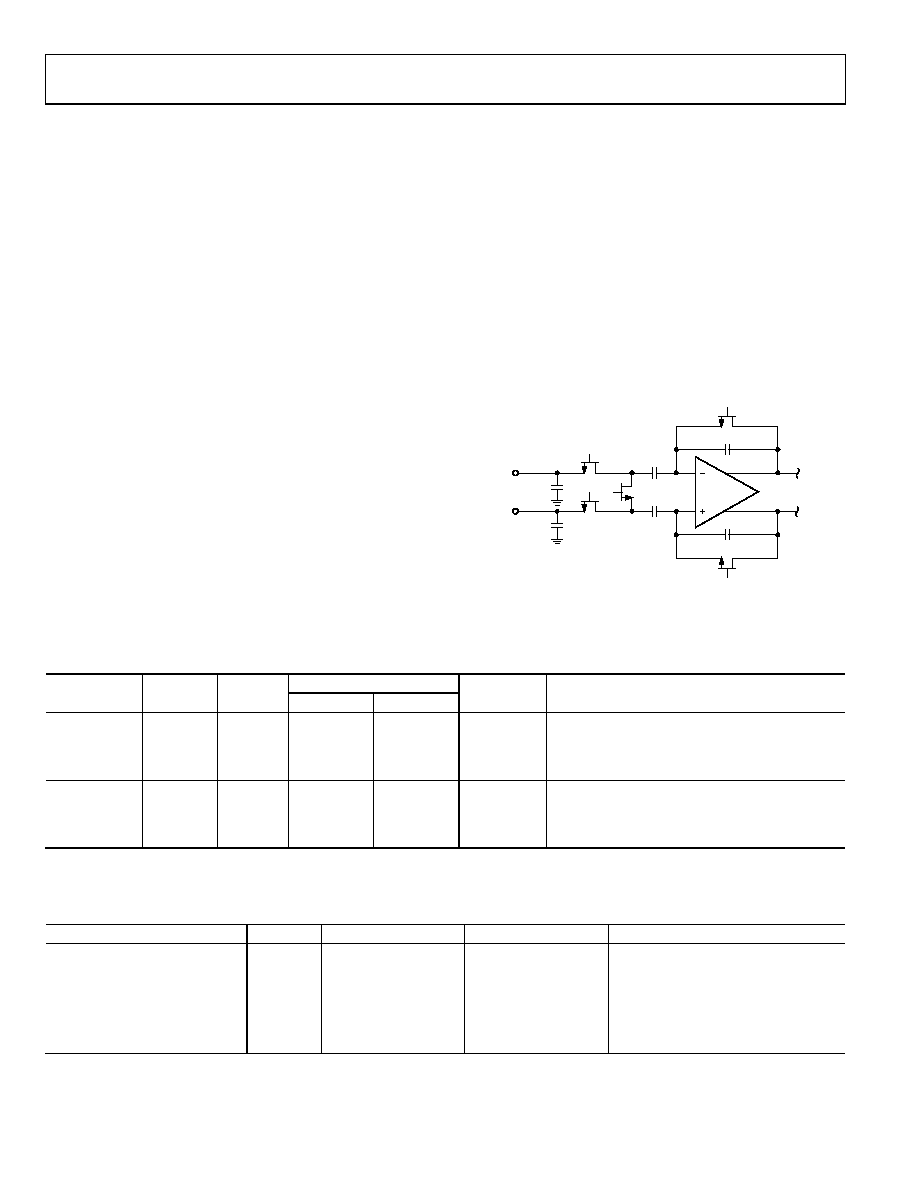
Figure 44 shows the equivalent analog input of the AD9244,
which consists of a 750 MHz differential SHA. The differential
input structure of the SHA is flexible, allowing the device to be
configured for either a differential or single-ended input. The
analog inputs VIN+ and VIN– are interchangeable, with the
exception that reversing the inputs to the VIN+ and VIN– pins
results in a data inversion (complementing the output word).
S
VIN+
VIN–
CPIN, PAR
S
H
CS
CH
CPIN, PAR
S
CH
02404-044
Figure 44. Analog Input of AD9244 SHA
Table 8. Analog Input Configuration Summary
Input
Input Range (V)
Input CM
Connection
Coupling
Span (V)
VIN+1
Voltage (V)
Comments
Single-Ended
DC or AC
1.0
0.5 to 1.5
1.0
Best for stepped input response applications.
2.0
1 to 3
2.0
Optimum noise performance for single-ended
mode often requires low distortion op amp
with VCC > 5 V due to its headroom issues.
Differential
DC or AC
1.0
2.25 to 2.75
2.75 to 2.25
2.5
Optimum full-scale THD and SFDR performance
well beyond the ADC’s Nyquist frequency.
2.0
2.0 to 3.0
3.0 to 2.0
2.5
Optimum noise performance for differential
mode. Preferred mode for applications.
1VIN+ and VIN can be interchanged if data inversion is required.
Table 9. Reference Configuration Summary
Reference Operating Mode
Connect
To
Resulting VREF (V)
Input Span (VIN+ VIN) (V p-p)
Internal
SENSE
VREF
1
Internal
SENSE
AGND
2
Internal
R1
VREF and SENSE
1 ≤ VREF ≤ 2.0
1 ≤ SPAN ≤ 2
R2
SENSE and REFGND
VREF = (1 + R1/R2)
(SPAN = VREF)
External
SENSE
AVDD
1 ≤ VREF ≤ 2.0
SPAN = EXTERNAL REF
VREF
EXTERNAL REF
相关PDF资料 |
PDF描述 |
|---|---|
| IDT7201LA12J | IC MEM FIFO 512X9 12NS 32-PLCC |
| MS3126E14-5P | CONN PLUG 5POS STRAIGHT W/PINS |
| AD7665ACPZRL | IC ADC 16BIT CMOS 5V 48LFCSP |
| LTC2858CMS-2#PBF | IC TXRX RS485/RS422 10-MSOP |
| VE-2T1-MY | CONVERTER MOD DC/DC 12V 50W |
相关代理商/技术参数 |
参数描述 |
|---|---|
| AD9244BSTZRL-401 | 制造商:AD 制造商全称:Analog Devices 功能描述:14-Bit, 40 MSPS/65 MSPS A/D Converter |
| AD9244BSTZRL-65 | 功能描述:IC ADC 14BIT SGL 65MSPS 48LQFP RoHS:是 类别:集成电路 (IC) >> 数据采集 - 模数转换器 系列:- 标准包装:1 系列:- 位数:14 采样率(每秒):83k 数据接口:串行,并联 转换器数目:1 功率耗散(最大):95mW 电压电源:双 ± 工作温度:0°C ~ 70°C 安装类型:通孔 封装/外壳:28-DIP(0.600",15.24mm) 供应商设备封装:28-PDIP 包装:管件 输入数目和类型:1 个单端,双极 |
| AD9244BSTZRL-651 | 制造商:AD 制造商全称:Analog Devices 功能描述:14-Bit, 40 MSPS/65 MSPS A/D Converter |
| AD9244-EVAL | 制造商:AD 制造商全称:Analog Devices 功能描述:14-Bit, 40/65 MSPS Monolithic A/D Converter |
| AD9245 | 制造商:AD 制造商全称:Analog Devices 功能描述:14-Bit, 80 MSPS, 3 V A/D Converter |
发布紧急采购,3分钟左右您将得到回复。