- 您现在的位置:买卖IC网 > PDF目录10211 > AD9245BCPZRL7-20 (Analog Devices Inc)IC ADC 14BIT SGL 20MSPS 32LFCSP PDF资料下载
参数资料
| 型号: | AD9245BCPZRL7-20 |
| 厂商: | Analog Devices Inc |
| 文件页数: | 13/32页 |
| 文件大小: | 0K |
| 描述: | IC ADC 14BIT SGL 20MSPS 32LFCSP |
| 标准包装: | 1,500 |
| 位数: | 14 |
| 采样率(每秒): | 20M |
| 数据接口: | 并联 |
| 转换器数目: | 3 |
| 功率耗散(最大): | 90mW |
| 电压电源: | 单电源 |
| 工作温度: | -40°C ~ 85°C |
| 安装类型: | 表面贴装 |
| 封装/外壳: | 32-VFQFN 裸露焊盘,CSP |
| 供应商设备封装: | 32-LFCSP-VQ(5x5) |
| 包装: | 带卷 (TR) |
| 输入数目和类型: | 2 个单端,单极;1 个差分,单极 |
第1页第2页第3页第4页第5页第6页第7页第8页第9页第10页第11页第12页当前第13页第14页第15页第16页第17页第18页第19页第20页第21页第22页第23页第24页第25页第26页第27页第28页第29页第30页第31页第32页
AD9245
Data Sheet
Rev. E | Page 20 of 32
JITTER CONSIDERATIONS
High speed, high resolution ADCs are sensitive to the quality
of the clock input. The degradation in SNR at a given input
frequency (fINPUT) due only to aperture jitter (tJ) can be
calculated with the following equation:
SNR = 20log10[2π fINPUT × tj]
In the equation, the rms aperture jitter represents the root-
mean square of all jitter sources, which include the clock input,
analog input signal, and ADC aperture jitter specification. IF
undersampling applications are particularly sensitive to jitter
The clock input should be treated as an analog signal in cases
where aperture jitter can affect the dynamic range of the
AD9245. Power supplies for clock drivers should be separated
from the ADC output driver supplies to avoid modulating the
clock signal with digital noise. Low jitter, crystal-controlled
oscillators make the best clock sources. If the clock is generated
from another type of source (by gating, dividing, or other
methods), it should be retimed by the original clock at the last step.
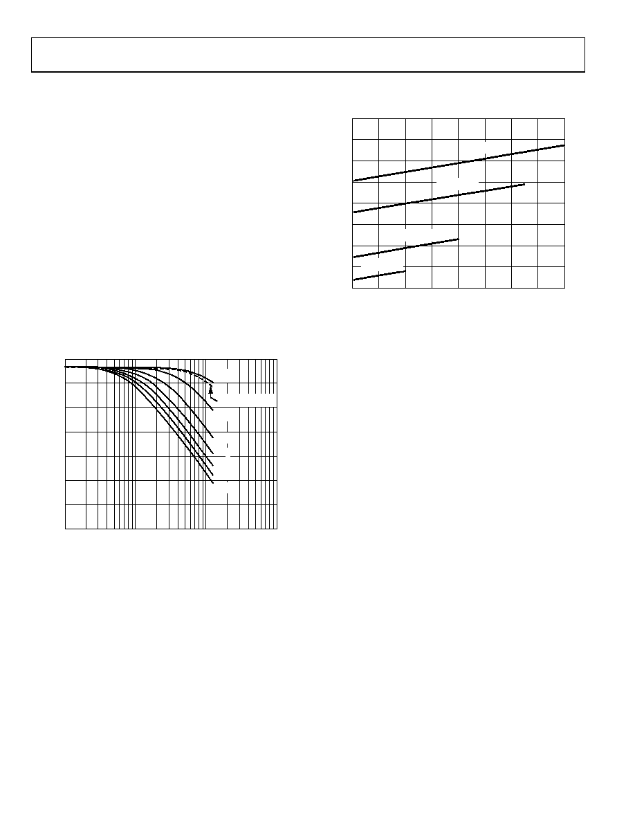
INPUT FREQUENCY (MHz)
SNR
(dBc)
1
40
75
70
65
60
55
50
45
1000
100
10
03583-
041
0.2ps
MEASURED SNR
0.5ps
1.0ps
1.5ps
2.0ps
2.5ps
3.0ps
Figure 43. SNR vs. Input Frequency and Jitter
POWER DISSIPATION AND STANDBY MODE
As shown in Figure 44, the power dissipated by the AD9245 is
proportional to its sample rate. The digital power dissipation is
determined primarily by the strength of the digital drivers and
the load on each output bit. The maximum DRVDD current
(IDRVDD) can be calculated as
N
f
C
V
I
CLK
LOAD
DRVDD
where N is the number of output bits, 14 in the case of the
AD9245. This maximum current occurs when every output bit
switches on every clock cycle, that is, a full-scale square wave at
the Nyquist frequency, fCLK/2. In practice, the DRVDD current
is established by the average number of output bits switching,
which is determined by the sample rate and the characteristics
of the analog input signal.
450
400
350
300
250
200
150
100
50
TOTAL
P
O
WE
R
(mW)
03583-074
0
1020
3040
50
607080
SAMPLE RATE (MSPS)
AD9245-80
AD9245-65
AD9245-40
AD9245-20
Figure 44. AD9245 Power vs. Sample Rate @ 2.5 MHz
Reducing the capacitive load presented to the output drivers can
minimize digital power consumption. The data in Figure 44 was
taken with the same operating conditions as those reported in
the Typical Performance Characteristics section, and with a
5 pF load on each output driver.
By asserting the PDWN pin high, the AD9245 is placed in
standby mode. In this state, the ADC typically dissipates
1 mW if the CLK and analog inputs are static. During standby,
the output drivers are placed in a high impedance state.
Reasserting the PDWN pin low returns the AD9245 to its
normal operational mode.
Low power dissipation in standby mode is achieved by shutting
down the reference, reference buffer, and biasing networks. The
decoupling capacitors on REFT and REFB are discharged when
entering standby mode and then must be recharged when
returning to normal operation. As a result, the wake-up time is
related to the time spent in standby mode, and shorter standby
cycles result in proportionally shorter wake-up times. With the
recommended 0.1 μF and 10 μF decoupling capacitors on REFT
and REFB, it takes approximately 1 second to fully discharge the
reference buffer decoupling capacitors and 7 ms to restore full
operation.
DIGITAL OUTPUTS
The AD9245 output drivers can be configured to interface with
2.5 V or 3.3 V logic families by matching DRVDD to the digital
supply of the interfaced logic. The output drivers are sized to
provide sufficient output current to drive a wide variety of logic
families. However, large drive currents tend to cause current
glitches on the supplies, which can affect converter performance.
Applications requiring the ADC to drive large capacitive loads or
large fanouts can require external buffers or latches.
相关PDF资料 |
PDF描述 |
|---|---|
| MS27466T19B32S | CONN RCPT 32POS WALL MT W/SCKT |
| SF7281-4PG-3ES | CONN RCPT 4POS PNL MNT PIN |
| D38999/24FC8PE | CONN RCPT 8POS JAM NUT W/PINS |
| SF7281-3SG-3ES | CONN RCPT 3POS PNL MNT SKT |
| MS3100C2422S | CONN RCPT 4POS WALL MNT W/SCKT |
相关代理商/技术参数 |
参数描述 |
|---|---|
| AD9245BCPZRL7-202 | 制造商:AD 制造商全称:Analog Devices 功能描述:14-Bit, 20 MSPS/40 MSPS/65 MSPS/80 MSPS, 3 V A/D Converter |
| AD9245BCPZRL7-40 | 功能描述:IC ADC 14BIT SGL 40MSPS 32LFCSP RoHS:是 类别:集成电路 (IC) >> 数据采集 - 模数转换器 系列:- 标准包装:1,000 系列:- 位数:12 采样率(每秒):300k 数据接口:并联 转换器数目:1 功率耗散(最大):75mW 电压电源:单电源 工作温度:0°C ~ 70°C 安装类型:表面贴装 封装/外壳:24-SOIC(0.295",7.50mm 宽) 供应商设备封装:24-SOIC 包装:带卷 (TR) 输入数目和类型:1 个单端,单极;1 个单端,双极 |
| AD9245BCPZRL7-402 | 制造商:AD 制造商全称:Analog Devices 功能描述:14-Bit, 20 MSPS/40 MSPS/65 MSPS/80 MSPS, 3 V A/D Converter |
| AD9245BCPZRL7-65 | 功能描述:IC ADC 14BIT SGL 65MSPS 32LFCSP RoHS:是 类别:集成电路 (IC) >> 数据采集 - 模数转换器 系列:- 标准包装:1 系列:- 位数:14 采样率(每秒):83k 数据接口:串行,并联 转换器数目:1 功率耗散(最大):95mW 电压电源:双 ± 工作温度:0°C ~ 70°C 安装类型:通孔 封装/外壳:28-DIP(0.600",15.24mm) 供应商设备封装:28-PDIP 包装:管件 输入数目和类型:1 个单端,双极 |
| AD9245BCPZRL7-652 | 制造商:AD 制造商全称:Analog Devices 功能描述:14-Bit, 20 MSPS/40 MSPS/65 MSPS/80 MSPS, 3 V A/D Converter |
发布紧急采购,3分钟左右您将得到回复。