- 您现在的位置:买卖IC网 > PDF目录10524 > AD9246BCPZ-80 (Analog Devices Inc)IC ADC 14BIT 80MSPS 48-LFCSP PDF资料下载
参数资料
| 型号: | AD9246BCPZ-80 |
| 厂商: | Analog Devices Inc |
| 文件页数: | 14/44页 |
| 文件大小: | 0K |
| 描述: | IC ADC 14BIT 80MSPS 48-LFCSP |
| 设计资源: | Using AD8376 to Drive Wide Bandwidth ADCs for High IF AC-Coupled Appls (CN0002) Driving AD9233/46/54 ADCs in AC-Coupled Baseband Appls (CN0051) |
| 标准包装: | 1 |
| 位数: | 14 |
| 采样率(每秒): | 80M |
| 数据接口: | 串行,SPI? |
| 转换器数目: | 3 |
| 功率耗散(最大): | 279mW |
| 电压电源: | 单电源 |
| 工作温度: | -40°C ~ 85°C |
| 安装类型: | 表面贴装 |
| 封装/外壳: | 48-VFQFN 裸露焊盘,CSP |
| 供应商设备封装: | 48-LFCSP-VQ(7x7) |
| 包装: | 托盘 |
| 输入数目和类型: | 2 个单端,单极;1 个差分,单极 |
第1页第2页第3页第4页第5页第6页第7页第8页第9页第10页第11页第12页第13页当前第14页第15页第16页第17页第18页第19页第20页第21页第22页第23页第24页第25页第26页第27页第28页第29页第30页第31页第32页第33页第34页第35页第36页第37页第38页第39页第40页第41页第42页第43页第44页
AD9246
Rev. A | Page 21 of 44
290
215
0
CLOCK FREQUENCY (MSPS)
P
O
WE
R
(
m
W)
150
0
CU
RRE
NT
(
m
A)
120
90
60
30
80
IDRVDD
IAVDD
TOTAL POWER
05
49
1-
0
91
275
260
245
230
20
40
60
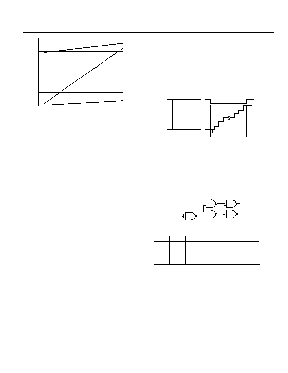
Figure 54. AD9246-80 Power and Current vs. Clock Frequency fIN = 30 MHz
Power-Down Mode
By asserting the PDWN pin high, the AD9246 is placed in
power-down mode. In this state, the ADC typically dissipates
1.8 mW. During power-down, the output drivers are placed in
a high impedance state. Reasserting the PDWN pin low returns
the AD9246 to its normal operational mode. This pin is both
1.8 V and 3.3 V tolerant.
Low power dissipation in power-down mode is achieved by
shutting down the reference, reference buffer, biasing networks,
and clock. The decoupling capacitors on REFT and REFB are
discharged when entering power-down mode and then must be
recharged when returning to normal operation. As a result, the
wake-up time is related to the time spent in power-down mode;
and shorter power-down cycles result in proportionally shorter
wake-up times. With the recommended 0.1 μF decoupling
capacitors on REFT and REFB, it takes approximately 0.25 ms
to fully discharge the reference buffer decoupling capacitors and
0.35 ms to restore full operation.
Standby Mode
When using the SPI port interface, the user can place the ADC
in power-down mode or standby mode. Standby mode allows the
user to keep the internal reference circuitry powered when
faster wake-up times are required (see the Memory Map section).
DIGITAL OUTPUTS
The AD9246 output drivers can be configured to interface with
1.8 V to 3.3 V logic families by matching DRVDD to the digital
supply of the interfaced logic. The output drivers are sized to
provide sufficient output current to drive a wide variety of logic
families. However, large drive currents tend to cause current
glitches on the supplies that may affect converter performance.
Applications requiring the ADC to drive large capacitive loads
or large fan-outs may require external buffers or latches.
The output data format can be selected for either offset binary
or twos complement by setting the SCLK/DFS pin when operat-
ing in the external pin mode (see Table 10).
As detailed in the Interfacing to High Speed ADCs via SPI User
Manual, the data format can be selected for either offset binary,
twos complement, or Gray code when using the SPI control.
Out-of-Range (OR) Condition
An out-of-range condition exists when the analog input voltage
is beyond the input range of the ADC. OR is a digital output
that is updated along with the data output corresponding to the
particular sampled input voltage. Thus, OR has the same pipeline
latency as the digital data.
05
49
1-
0
88
1
0
1
OR DATA OUTPUTS
OR
+FS – 1 LSB
+FS – 1/2 LSB
+FS
–FS
–FS + 1/2 LSB
–FS – 1/2 LSB
1111
1110
0000
11
00
0000
0001
0000
Figure 55. OR Relation to Input Voltage and Output Data
OR is low when the analog input voltage is within the analog
input range and high when the analog input voltage exceeds the
input range, as shown in Figure 55. OR remains high until the
analog input returns to within the input range, and another conver-
sion is completed. By logically AND’ing the OR bit with the MSB
and its complement, overrange high or underrange low conditions
can be detected. Table 11 is a truth table for the overrange/
underrange circuit in Figure 56, which uses NAND gates.
MSB
OR
MSB
OVER = 1
UNDER = 1
05
49
1-
0
8
7
Figure 56. Overrange/Underrange Logic
Table 11. Overrange/Underrange Truth Table
OR
MSB
Analog Input Is:
0
Within range
0
1
Within range
1
0
Underrange
1
Overrange
Digital Output Enable Function (OEB)
The AD9246 has three-state ability. If the OEB pin is low, the
output data drivers are enabled. If the OEB pin is high, the
output data drivers are placed in a high impedance state. This is
not intended for rapid access to the data bus. Note that OEB is
referenced to the digital supplies (DRVDD) and should not
exceed that supply voltage.
相关PDF资料 |
PDF描述 |
|---|---|
| SSM2301CPZ-REEL7 | IC AMP AUDIO 1.52W MONO D 8LFCSP |
| AD9284BCPZ-250 | IC ADC 8BIT 250MSPS 1.8V 48LFCSP |
| AD9649BCPZ-80 | IC ADC 14BIT 80MSPS 32LFCSP |
| AD9627ABCPZ11-105 | IC ADC 11BIT 105MSPS 64LFCSP |
| AD7876BNZ | IC ADC 12BIT SAMPLING 10V 24DIP |
相关代理商/技术参数 |
参数描述 |
|---|---|
| AD9246BCPZRL7-105 | 功能描述:IC ADC 14BIT 105MSPS 48-LFCSP RoHS:是 类别:集成电路 (IC) >> 数据采集 - 模数转换器 系列:- 标准包装:1 系列:- 位数:14 采样率(每秒):83k 数据接口:串行,并联 转换器数目:1 功率耗散(最大):95mW 电压电源:双 ± 工作温度:0°C ~ 70°C 安装类型:通孔 封装/外壳:28-DIP(0.600",15.24mm) 供应商设备封装:28-PDIP 包装:管件 输入数目和类型:1 个单端,双极 |
| AD9246BCPZRL7-125 | 功能描述:IC ADC 14BIT 125MSPS 48-LFCSP RoHS:是 类别:集成电路 (IC) >> 数据采集 - 模数转换器 系列:- 标准包装:1 系列:- 位数:14 采样率(每秒):83k 数据接口:串行,并联 转换器数目:1 功率耗散(最大):95mW 电压电源:双 ± 工作温度:0°C ~ 70°C 安装类型:通孔 封装/外壳:28-DIP(0.600",15.24mm) 供应商设备封装:28-PDIP 包装:管件 输入数目和类型:1 个单端,双极 |
| AD9246BCPZRL7-80 | 制造商:Analog Devices 功能描述:14-BIT, 80 MSPS/105 MSPS/125 MSPS, 1.8 V ANALOG-TO-DIGITAL C - Tape and Reel |
| AD9248 | 制造商:Analog Devices 功能描述:40 MSPS DUAL A/D CONVERTER - Bulk |
| AD9248-20PCB | 制造商:AD 制造商全称:Analog Devices 功能描述:14-Bit, 20/40/65 MSPS Dual A/ D Converter |
发布紧急采购,3分钟左右您将得到回复。