- 您现在的位置:买卖IC网 > PDF目录10524 > AD9246BCPZ-80 (Analog Devices Inc)IC ADC 14BIT 80MSPS 48-LFCSP PDF资料下载
参数资料
| 型号: | AD9246BCPZ-80 |
| 厂商: | Analog Devices Inc |
| 文件页数: | 17/44页 |
| 文件大小: | 0K |
| 描述: | IC ADC 14BIT 80MSPS 48-LFCSP |
| 设计资源: | Using AD8376 to Drive Wide Bandwidth ADCs for High IF AC-Coupled Appls (CN0002) Driving AD9233/46/54 ADCs in AC-Coupled Baseband Appls (CN0051) |
| 标准包装: | 1 |
| 位数: | 14 |
| 采样率(每秒): | 80M |
| 数据接口: | 串行,SPI? |
| 转换器数目: | 3 |
| 功率耗散(最大): | 279mW |
| 电压电源: | 单电源 |
| 工作温度: | -40°C ~ 85°C |
| 安装类型: | 表面贴装 |
| 封装/外壳: | 48-VFQFN 裸露焊盘,CSP |
| 供应商设备封装: | 48-LFCSP-VQ(7x7) |
| 包装: | 托盘 |
| 输入数目和类型: | 2 个单端,单极;1 个差分,单极 |
第1页第2页第3页第4页第5页第6页第7页第8页第9页第10页第11页第12页第13页第14页第15页第16页当前第17页第18页第19页第20页第21页第22页第23页第24页第25页第26页第27页第28页第29页第30页第31页第32页第33页第34页第35页第36页第37页第38页第39页第40页第41页第42页第43页第44页
AD9246
Rev. A | Page 24 of 44
MEMORY MAP
READING THE MEMORY MAP REGISTER TABLE
Each row in the memory map register table has eight address
locations. The memory map is roughly divided into three
sections: the chip configuration registers map (Address 0x00 to
Address 0x02), the device index and transfer registers map
(Address 0xFF), and the ADC functions map (Address 0x08 to
Address 0x18).
Table 15 displays the register address number in hexadecimal in
the first column. The last column displays the default value for
each hexadecimal address. The Bit 7 (MSB) column is the start
of the default hexadecimal value given. For example, Hexadecimal
Address 0x14, output_phase, has a hexadecimal default value of
0x00. This means Bit 3 = 0, Bit 2 = 0, Bit 1 = 1, and Bit 0 = 1 or
0011 in binary. This setting is the default output clock or DCO
phase adjust option. The default value adjusts the DCO phase
90° relative to the nominal DCO edge and 180° relative to the
data edge. For more information on this function, consult the
Open Locations
Locations marked as open are currently not supported for this
device. When required, these locations should be written with
0s. Writing to these locations is required only when part of an
address location is open (for example, Address 0x14). If the
entire address location is open (Address 0x13), then the address
location does not need to be written.
Default Values
Coming out of reset, critical registers are loaded with default
values. The default values for the registers are shown in Table 15.
Logic Levels
An explanation of two registers follows:
“Bit is set” is synonymous with “Bit is set to Logic 1” or
“Writing Logic 1 for the bit.”
“Clear a bit” is synonymous with “Bit is set to Logic 0” or
“Writing Logic 0 for the bit.”
SPI-Accessible Features
A list of features accessible via the SPI and a brief description of
what the user can do with these features follow. These features
are described in detail in the Interfacing to High Speed ADCs via
Modes:
Set either power-down or standby mode.
Clock:
Access the DCS via the SPI.
Offset:
Digitally adjust the converter offset.
Test I/O:
Set test modes to have known data on output bits.
Output Mode:
Set up outputs; vary the strength of the
output drivers.
Output Phase:
Set the output clock polarity.
VREF:
Set the reference voltage.
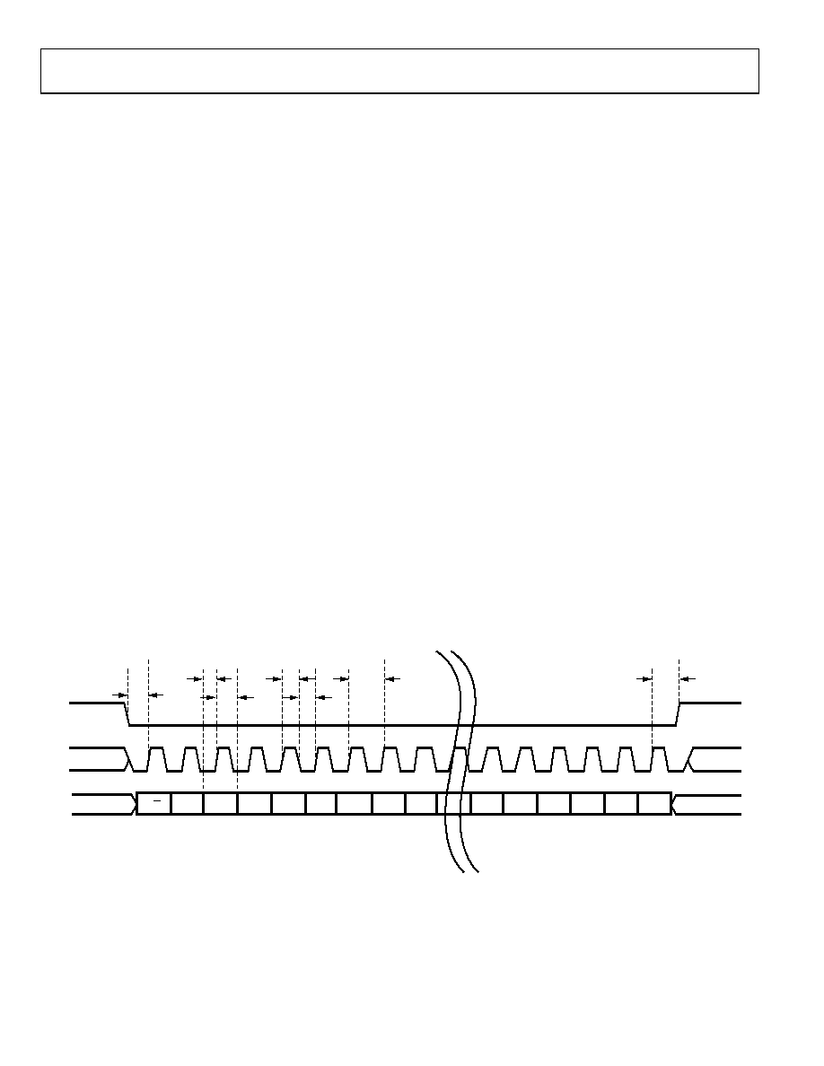
DON’T CARE
SDIO
SCLK
CSB
tS
tDH
tHI
tCLK
tLO
tDS
tH
R/W
W1
W0
A12
A11
A10
A9
A8
A7
D5
D4
D3
D2
D1
D0
05491-
0
56
Figure 57. Serial Port Interface Timing Diagram
相关PDF资料 |
PDF描述 |
|---|---|
| SSM2301CPZ-REEL7 | IC AMP AUDIO 1.52W MONO D 8LFCSP |
| AD9284BCPZ-250 | IC ADC 8BIT 250MSPS 1.8V 48LFCSP |
| AD9649BCPZ-80 | IC ADC 14BIT 80MSPS 32LFCSP |
| AD9627ABCPZ11-105 | IC ADC 11BIT 105MSPS 64LFCSP |
| AD7876BNZ | IC ADC 12BIT SAMPLING 10V 24DIP |
相关代理商/技术参数 |
参数描述 |
|---|---|
| AD9246BCPZRL7-105 | 功能描述:IC ADC 14BIT 105MSPS 48-LFCSP RoHS:是 类别:集成电路 (IC) >> 数据采集 - 模数转换器 系列:- 标准包装:1 系列:- 位数:14 采样率(每秒):83k 数据接口:串行,并联 转换器数目:1 功率耗散(最大):95mW 电压电源:双 ± 工作温度:0°C ~ 70°C 安装类型:通孔 封装/外壳:28-DIP(0.600",15.24mm) 供应商设备封装:28-PDIP 包装:管件 输入数目和类型:1 个单端,双极 |
| AD9246BCPZRL7-125 | 功能描述:IC ADC 14BIT 125MSPS 48-LFCSP RoHS:是 类别:集成电路 (IC) >> 数据采集 - 模数转换器 系列:- 标准包装:1 系列:- 位数:14 采样率(每秒):83k 数据接口:串行,并联 转换器数目:1 功率耗散(最大):95mW 电压电源:双 ± 工作温度:0°C ~ 70°C 安装类型:通孔 封装/外壳:28-DIP(0.600",15.24mm) 供应商设备封装:28-PDIP 包装:管件 输入数目和类型:1 个单端,双极 |
| AD9246BCPZRL7-80 | 制造商:Analog Devices 功能描述:14-BIT, 80 MSPS/105 MSPS/125 MSPS, 1.8 V ANALOG-TO-DIGITAL C - Tape and Reel |
| AD9248 | 制造商:Analog Devices 功能描述:40 MSPS DUAL A/D CONVERTER - Bulk |
| AD9248-20PCB | 制造商:AD 制造商全称:Analog Devices 功能描述:14-Bit, 20/40/65 MSPS Dual A/ D Converter |
发布紧急采购,3分钟左右您将得到回复。