- 您现在的位置:买卖IC网 > PDF目录10652 > AD9253BCPZ-125 (Analog Devices Inc)IC ADC 14BIT SRL 125MSPS 48LFCSP PDF资料下载
参数资料
| 型号: | AD9253BCPZ-125 |
| 厂商: | Analog Devices Inc |
| 文件页数: | 16/40页 |
| 文件大小: | 0K |
| 描述: | IC ADC 14BIT SRL 125MSPS 48LFCSP |
| 标准包装: | 1 |
| 位数: | 14 |
| 采样率(每秒): | 125M |
| 数据接口: | LVDS,串行,SPI? |
| 转换器数目: | 4 |
| 功率耗散(最大): | 540mW |
| 电压电源: | 模拟和数字 |
| 工作温度: | -40°C ~ 85°C |
| 安装类型: | 表面贴装 |
| 封装/外壳: | 48-WFQFN 裸露焊盘,CSP |
| 供应商设备封装: | 48-LFCSP-WQ(7x7) |
| 包装: | 托盘 |
| 输入数目和类型: | 4 个差分,双极 |
第1页第2页第3页第4页第5页第6页第7页第8页第9页第10页第11页第12页第13页第14页第15页当前第16页第17页第18页第19页第20页第21页第22页第23页第24页第25页第26页第27页第28页第29页第30页第31页第32页第33页第34页第35页第36页第37页第38页第39页第40页
Data Sheet
AD9253
Rev. 0 | Page 23 of 40
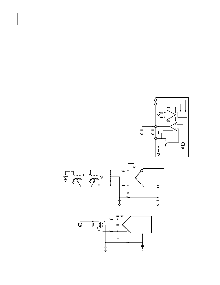
Differential Input Configurations
There are several ways to drive the AD9253 either actively or
passively. However, optimum performance is achieved by driving
the analog inputs differentially. Using a differential double balun
configuration to drive the AD9253 provides excellent performance
and a flexible interface to the ADC (see Figure 58) for baseband
applications.
For applications where SNR is a key parameter, differential trans-
former coupling is the recommended input configuration (see
Figure 59), because the noise performance of most amplifiers is
not adequate to achieve the true performance of the AD9253.
Regardless of the configuration, the value of the shunt capacitor,
C, is dependent on the input frequency and may need to be
reduced or removed.
It is not recommended to drive the AD9253 inputs single-ended.
VOLTAGE REFERENCE
A stable and accurate 1.0 V voltage reference is built into the
AD9253. VREF can be configured using either the internal 1.0 V
reference or an externally applied 1.0 V reference voltage. The
various reference modes are summarized in the Internal Reference
Connection section and the External Reference Operation
section. The VREF pin should be externally decoupled to
ground with a low ESR, 1.0 μF capacitor in parallel with a low
ESR, 0.1 μF ceramic capacitor.
Internal Reference Connection
A comparator within the AD9253 detects the potential at the
SENSE pin and configures the reference into two possible
modes, which are summarized in Table 9. If SENSE is grounded,
the reference amplifier switch is connected to the internal resistor
divider (see Figure 57), setting VREF to 1.0 V.
Table 9. Reference Configuration Summary
Selected Mode
SENSE
Voltage (V)
Resulting
VREF (V)
Resulting
Differential
Span (V p-p)
Fixed Internal
Reference
AGND to
0.2
1.0 internal
2.0
Fixed External
Reference
AVDD
1.0 applied
to external
VREF pin
2.0
VREF
SENSE
0.5V
ADC
SELECT
LOGIC
0.1F
1.0F
VIN–A/VIN–B
VIN+A/VIN+B
ADC
CORE
10
06
5-
06
0
Figure 57. Internal Reference Configuration
ADC
R
0.1F
2V p-p
VCM
C
*C1
C
R
0.1F
33
200
33
VIN+x
VIN–x
100
65-
059
ET1-1-I3
C
5pF
R
*C1 IS OPTIONAL
Figure 58. Differential Double Balun Input Configuration for Baseband Applications
2V p-p
R
*C1
*C1 IS OPTIONAL
49.9
0.1μF
ADT1-1WT
1:1 Z RATIO
VIN–x
ADC
VIN+x
*C1
C
VCM
10
065-
05
6
33
200
0.1F
5pF
Figure 59. Differential Transformer-Coupled Configuration
for Baseband Applications
相关PDF资料 |
PDF描述 |
|---|---|
| LTC2284IUP#PBF | IC ADC DUAL 14BIT 105MSPS 64-QFN |
| VE-211-IW-F4 | CONVERTER MOD DC/DC 12V 100W |
| LTC2172IUKG-14#PBF | IC ADC 14BIT SER/PAR 65M 52-QFN |
| VI-JTN-MY-F4 | CONVERTER MOD DC/DC 18.5V 50W |
| MAX970EEE+T | IC COMPARATOR R-R 16-QSOP |
相关代理商/技术参数 |
参数描述 |
|---|---|
| AD9253BCPZ-80 | 功能描述:IC ADC 14BIT SRL 80MSPS 48LFCSP RoHS:是 类别:集成电路 (IC) >> 数据采集 - 模数转换器 系列:- 其它有关文件:TSA1204 View All Specifications 标准包装:1 系列:- 位数:12 采样率(每秒):20M 数据接口:并联 转换器数目:2 功率耗散(最大):155mW 电压电源:模拟和数字 工作温度:-40°C ~ 85°C 安装类型:表面贴装 封装/外壳:48-TQFP 供应商设备封装:48-TQFP(7x7) 包装:Digi-Reel® 输入数目和类型:4 个单端,单极;2 个差分,单极 产品目录页面:1156 (CN2011-ZH PDF) 其它名称:497-5435-6 |
| AD9253BCPZRL7-105 | 功能描述:模数转换器 - ADC 14 Bit 105Msps Quad ADC RoHS:否 制造商:Analog Devices 通道数量: 结构: 转换速率: 分辨率: 输入类型: 信噪比: 接口类型: 工作电源电压: 最大工作温度: 安装风格: 封装 / 箱体: |
| AD9253BCPZRL7-125 | 功能描述:模数转换器 - ADC 14 Bit 125Msps Quad ADC RoHS:否 制造商:Analog Devices 通道数量: 结构: 转换速率: 分辨率: 输入类型: 信噪比: 接口类型: 工作电源电压: 最大工作温度: 安装风格: 封装 / 箱体: |
| AD9253BCPZRL7-80 | 功能描述:模数转换器 - ADC 14 Bit 80 Msps Quad ADC RoHS:否 制造商:Analog Devices 通道数量: 结构: 转换速率: 分辨率: 输入类型: 信噪比: 接口类型: 工作电源电压: 最大工作温度: 安装风格: 封装 / 箱体: |
| AD9253TCPZ-125EP | 功能描述:IC ADC 14BIT SRL 125MSPS 48LFCSP RoHS:是 类别:集成电路 (IC) >> 数据采集 - 模数转换器 系列:- 产品培训模块:Lead (SnPb) Finish for COTS Obsolescence Mitigation Program 标准包装:250 系列:- 位数:12 采样率(每秒):1.8M 数据接口:并联 转换器数目:1 功率耗散(最大):1.82W 电压电源:模拟和数字 工作温度:-40°C ~ 85°C 安装类型:表面贴装 封装/外壳:48-LQFP 供应商设备封装:48-LQFP(7x7) 包装:管件 输入数目和类型:2 个单端,单极 |
发布紧急采购,3分钟左右您将得到回复。