- 您现在的位置:买卖IC网 > PDF目录9471 > AD9273BBCZ-25 (Analog Devices Inc)IC ADCASD OCTAL 25MSPS 144CSPBGA PDF资料下载
参数资料
| 型号: | AD9273BBCZ-25 |
| 厂商: | Analog Devices Inc |
| 文件页数: | 15/48页 |
| 文件大小: | 0K |
| 描述: | IC ADCASD OCTAL 25MSPS 144CSPBGA |
| 标准包装: | 1 |
| 类型: | AAF,ADC,交叉点开关,LNA,VGA |
| 分辨率(位): | 12 b |
| 采样率(每秒): | 25M |
| 数据接口: | 串行,SPI? |
| 电压电源: | 模拟和数字 |
| 电源电压: | 1.8V,3V |
| 工作温度: | -40°C ~ 85°C |
| 安装类型: | 表面贴装 |
| 封装/外壳: | 144-LFBGA,CSPBGA |
| 供应商设备封装: | 144-CSPBGA(10x10) |
| 包装: | 托盘 |
第1页第2页第3页第4页第5页第6页第7页第8页第9页第10页第11页第12页第13页第14页当前第15页第16页第17页第18页第19页第20页第21页第22页第23页第24页第25页第26页第27页第28页第29页第30页第31页第32页第33页第34页第35页第36页第37页第38页第39页第40页第41页第42页第43页第44页第45页第46页第47页第48页
AD9273
Rev. B | Page 22 of 48
LNA
LI-x
LG-x
LO-x
DOUTx+
DOUTx–
CS
T/R
SWITCH
CLG
CFB R
FB2
CSH
GAIN
INTERPOLATOR
LOSW-x
RFB1
SWITCH
ARRAY
gm
CWD[7:0]+
CWD[7:0]–
ATTENUATOR
–42dB TO 0dB
GA
IN
–
PIPELINE
ADC
SERIAL
LVDS
POSTAMP
GA
IN
+
AD9273
T
RANS
DUCE
R
FILTER
21dB
24dB,
27dB,
30dB
15.6dB,
17.9dB,
21.3dB
07
03
0-
0
71
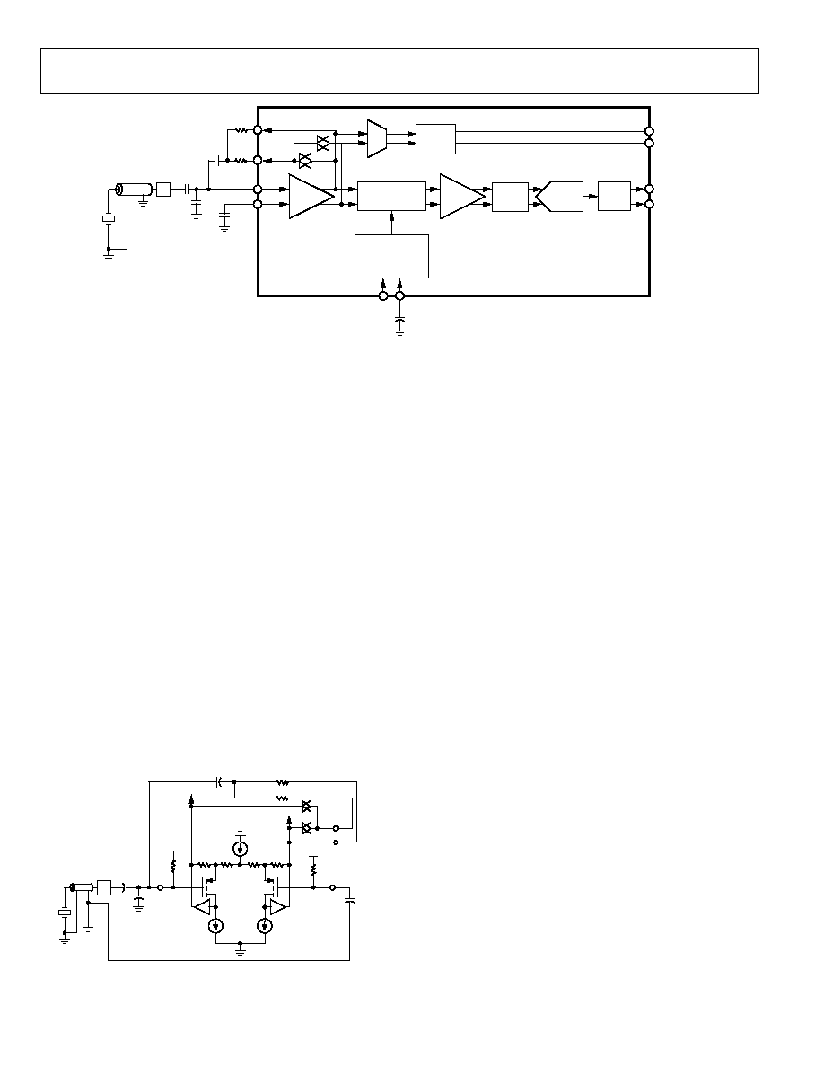
Figure 38. Simplified Block Diagram of a Single Channel
CHANNEL OVERVIEW
Each channel contains both a TGC signal path and a CW Doppler
signal path. Common to both signal paths, the LNA provides user-
adjustable input impedance termination. The CW Doppler path
includes a transconductance amplifier and a crosspoint switch.
The TGC path includes a differential X-AMP VGA, an antialiasing
filter, and an ADC. Figure 38 shows a simplified block diagram
with external components.
The signal path is fully differential throughout to maximize signal
swing and reduce even-order distortion; however, the LNA is
designed to be driven from a single-ended signal source.
Low Noise Amplifier (LNA)
Good noise performance relies on a proprietary ultralow noise
LNA at the beginning of the signal chain, which minimizes the
noise contribution in the following VGA. Active impedance
control optimizes noise performance for applications that benefit
from input impedance matching.
A simplified schematic of the LNA is shown in Figure 39. LI-x is
capacitively coupled to the source. An on-chip bias generator
establishes dc input bias voltages of around 0.9 V and centers
the output common-mode levels at 1.5 V (AVDD2 divided by
2). A capacitor, CLG, of the same value as the input coupling
capacitor, CS, is connected from the LG-x pin to ground.
LI-x
CS
CLG
CFB
CSH
LG-x
LO-x
LOSW-x
VCM
VO+
VO–
RFB1
RFB2
T/R
SWITCH
T
RANS
DUCE
R
07
03
0-
10
1
Figure 39. Simplified LNA Schematic
The LNA supports differential output voltages as high as
4.4 V p-p with positive and negative excursions of ±1.1 V from a
common-mode voltage of 1.5 V. The LNA differential gain sets
the maximum input signal before saturation. One of three gains
is set through the SPI. The corresponding full-scale input for
the gain settings of 6, 8, and 12 is 733 mV p-p, 550 mV p-p, and
367 mV p-p, respectively. Overload protection ensures quick
recovery time from large input voltages. Because the inputs are
capacitively coupled to a bias voltage near midsupply, very large
inputs can be handled without interacting with the ESD protection.
Low value feedback resistors and the current-driving capability
of the output stage allow the LNA to achieve a low input-referred
noise voltage of 1.26 nV/√Hz at a gain of 21.3 dB. This is achieved
with a current consumption of only 10 mA per channel (30 mW).
On-chip resistor matching results in precise single-ended gains,
which are critical for accurate impedance control. The use of a
fully differential topology and negative feedback minimizes
distortion. Low second-order harmonic distortion is particularly
important in second-order harmonic ultrasound imaging
applications. Differential signaling enables smaller swings at
each output, further reducing third-order distortion.
Recommendation
It is highly recommended that the LG-x pins form a Kelvin type
connection to the input or probe connection ground. Simply
connecting the LG pin to ground near the device may allow
differences in potential to be amplified through the LNA. This
generally shows up as a dc offset voltage that can vary from
channel to channel and part to part, depending on the
application and layout of the PCB (see Figure 38).
相关PDF资料 |
PDF描述 |
|---|---|
| LTC6905HS5-100#TRMPBF | IC OSC SILICON 100MHZ TSOT23-5 |
| AD9273BSVZ-25 | IC ADC OCT 12BIT 25MSPS 100-TQFP |
| LTC6905HS5-96#TRPBF | IC OSC SILICON 96MHZ TSOT23-5 |
| LTC6905HS5-80#TRPBF | IC OSC SILICON 80MHZ TSOT23-5 |
| AD7874BNZ | IC DAS 12BIT 4CH 5V 28-DIP |
相关代理商/技术参数 |
参数描述 |
|---|---|
| AD9273BBCZ-40 | 功能描述:IC ADCASD OCTAL 25MSPS 144CSPBGA RoHS:是 类别:集成电路 (IC) >> 数据采集 - ADCs/DAC - 专用型 系列:- 产品培训模块:Lead (SnPb) Finish for COTS Obsolescence Mitigation Program 标准包装:50 系列:- 类型:数据采集系统(DAS) 分辨率(位):16 b 采样率(每秒):21.94k 数据接口:MICROWIRE?,QSPI?,串行,SPI? 电压电源:模拟和数字 电源电压:1.8 V ~ 3.6 V 工作温度:-40°C ~ 85°C 安装类型:表面贴装 封装/外壳:40-WFQFN 裸露焊盘 供应商设备封装:40-TQFN-EP(6x6) 包装:托盘 |
| AD9273BBCZ-50 | 功能描述:IC ADCASD OCTAL 25MSPS 144CSPBGA RoHS:是 类别:集成电路 (IC) >> 数据采集 - ADCs/DAC - 专用型 系列:- 产品培训模块:Lead (SnPb) Finish for COTS Obsolescence Mitigation Program 标准包装:50 系列:- 类型:数据采集系统(DAS) 分辨率(位):16 b 采样率(每秒):21.94k 数据接口:MICROWIRE?,QSPI?,串行,SPI? 电压电源:模拟和数字 电源电压:1.8 V ~ 3.6 V 工作温度:-40°C ~ 85°C 安装类型:表面贴装 封装/外壳:40-WFQFN 裸露焊盘 供应商设备封装:40-TQFN-EP(6x6) 包装:托盘 |
| AD9273BSVZ-25 | 功能描述:IC ADC OCT 12BIT 25MSPS 100-TQFP RoHS:是 类别:集成电路 (IC) >> 数据采集 - ADCs/DAC - 专用型 系列:- 产品培训模块:Lead (SnPb) Finish for COTS Obsolescence Mitigation Program 标准包装:50 系列:- 类型:数据采集系统(DAS) 分辨率(位):16 b 采样率(每秒):21.94k 数据接口:MICROWIRE?,QSPI?,串行,SPI? 电压电源:模拟和数字 电源电压:1.8 V ~ 3.6 V 工作温度:-40°C ~ 85°C 安装类型:表面贴装 封装/外壳:40-WFQFN 裸露焊盘 供应商设备封装:40-TQFN-EP(6x6) 包装:托盘 |
| AD9273BSVZ-40 | 功能描述:IC ADC OCT 12BIT 40MSPS 100-TQFP RoHS:是 类别:集成电路 (IC) >> 数据采集 - ADCs/DAC - 专用型 系列:- 产品培训模块:Lead (SnPb) Finish for COTS Obsolescence Mitigation Program 标准包装:50 系列:- 类型:数据采集系统(DAS) 分辨率(位):16 b 采样率(每秒):21.94k 数据接口:MICROWIRE?,QSPI?,串行,SPI? 电压电源:模拟和数字 电源电压:1.8 V ~ 3.6 V 工作温度:-40°C ~ 85°C 安装类型:表面贴装 封装/外壳:40-WFQFN 裸露焊盘 供应商设备封装:40-TQFN-EP(6x6) 包装:托盘 |
| AD9273BSVZ-50 | 功能描述:IC ADC ASD OCTAL 50MSPS 100-TQFP RoHS:是 类别:集成电路 (IC) >> 数据采集 - ADCs/DAC - 专用型 系列:- 产品培训模块:Lead (SnPb) Finish for COTS Obsolescence Mitigation Program 标准包装:50 系列:- 类型:数据采集系统(DAS) 分辨率(位):16 b 采样率(每秒):21.94k 数据接口:MICROWIRE?,QSPI?,串行,SPI? 电压电源:模拟和数字 电源电压:1.8 V ~ 3.6 V 工作温度:-40°C ~ 85°C 安装类型:表面贴装 封装/外壳:40-WFQFN 裸露焊盘 供应商设备封装:40-TQFN-EP(6x6) 包装:托盘 |
发布紧急采购,3分钟左右您将得到回复。