- 您现在的位置:买卖IC网 > PDF目录9471 > AD9273BBCZ-25 (Analog Devices Inc)IC ADCASD OCTAL 25MSPS 144CSPBGA PDF资料下载
参数资料
| 型号: | AD9273BBCZ-25 |
| 厂商: | Analog Devices Inc |
| 文件页数: | 17/48页 |
| 文件大小: | 0K |
| 描述: | IC ADCASD OCTAL 25MSPS 144CSPBGA |
| 标准包装: | 1 |
| 类型: | AAF,ADC,交叉点开关,LNA,VGA |
| 分辨率(位): | 12 b |
| 采样率(每秒): | 25M |
| 数据接口: | 串行,SPI? |
| 电压电源: | 模拟和数字 |
| 电源电压: | 1.8V,3V |
| 工作温度: | -40°C ~ 85°C |
| 安装类型: | 表面贴装 |
| 封装/外壳: | 144-LFBGA,CSPBGA |
| 供应商设备封装: | 144-CSPBGA(10x10) |
| 包装: | 托盘 |
第1页第2页第3页第4页第5页第6页第7页第8页第9页第10页第11页第12页第13页第14页第15页第16页当前第17页第18页第19页第20页第21页第22页第23页第24页第25页第26页第27页第28页第29页第30页第31页第32页第33页第34页第35页第36页第37页第38页第39页第40页第41页第42页第43页第44页第45页第46页第47页第48页
AD9273
Rev. B | Page 24 of 48
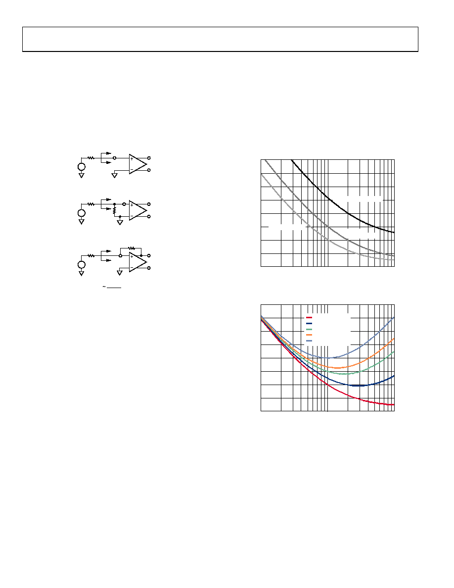
LNA Noise
The short-circuit noise voltage (input-referred noise) is an impor-
tant limit on system performance. The short-circuit input-referred
noise voltage for the LNA is 1.4 nV/√Hz at a gain of 21.3 dB,
including the VGA noise at a VGA postamp gain of 27 dB. These
measurements, which were taken without a feedback resistor,
provide the basis for calculating the input noise and noise figure
(NF) performance of the configurations shown in Figure 41.
VOUT
UNTERMINATED
+
–
LI-x
RIN
RS
VOUT
RESISTIVE TERMINATION
+
–
LI-x
RIN
RS
VOUT
ACTIVE IMPEDANCE MATCH
+
–
LI-x
RIN
RFB
1 + A/2
RS
RIN =
0
70
30
-10
4
Figure 41. Input Configurations
resistance (RS) results using these configurations and an input-
referred noise voltage of 6 nV/√Hz for the VGA. Unterminated
(RFB = ∞) operation exhibits the lowest equivalent input noise
low RS—where the LNA voltage noise is large compared with the
source noise—and at high RS due to the noise contribution from
RFB. The lowest NF is achieved when RS matches RIN.
The main purpose of input impedance matching is to improve the
transient response of the system. With resistive termination, the
input noise increases due to the thermal noise of the matching
resistor and the increased contribution of the LNA’s input
voltage noise generator. With active impedance matching,
however, the contributions of both are smaller (by a factor of
1/(1 + LNA Gain)) than they would be for resistive termination.
Figure 42 shows the relative noise figure performance. In this
graph, the input impedance was swept with RS to preserve the
match at each point. The noise figures for a source impedance of
50 Ω are 7.3 dB, 4.2 dB, and 2.8 dB for the resistive termination,
active termination, and unterminated configurations, respectively.
The noise figures for 200 Ω are 4.5 dB, 1.7 dB, and 1.0 dB,
respectively.
of RIN, which is helpful for design purposes.
10
100
1k
0
1.5
3.0
4.5
6.0
7.5
9.0
10.5
12.0
RS ()
NO
IS
E
F
IG
UR
E
(
d
B)
07
03
0-
18
2
UNTERMINATED
SHUNT TERMINATION
ACTIVE
TERMINATION
Figure 42. Noise Figure vs. RS for Shunt Termination,
Active Termination Matched, and Unterminated Inputs, VGAIN = 0.8 V
10
100
1k
0
1.5
3.0
4.5
6.0
7.5
9.0
10.5
12.0
RS ()
NO
IS
E
F
IG
UR
E
(
d
B)
07
03
0-
18
3
UNTERMINATED
RIN = 200
RIN = 100
RIN = 75
RIN = 50
Figure 43. Noise Figure vs. RS for Various Fixed Values of RIN,
Active Termination Matched Inputs, VGAIN = 0.8 V
相关PDF资料 |
PDF描述 |
|---|---|
| LTC6905HS5-100#TRMPBF | IC OSC SILICON 100MHZ TSOT23-5 |
| AD9273BSVZ-25 | IC ADC OCT 12BIT 25MSPS 100-TQFP |
| LTC6905HS5-96#TRPBF | IC OSC SILICON 96MHZ TSOT23-5 |
| LTC6905HS5-80#TRPBF | IC OSC SILICON 80MHZ TSOT23-5 |
| AD7874BNZ | IC DAS 12BIT 4CH 5V 28-DIP |
相关代理商/技术参数 |
参数描述 |
|---|---|
| AD9273BBCZ-40 | 功能描述:IC ADCASD OCTAL 25MSPS 144CSPBGA RoHS:是 类别:集成电路 (IC) >> 数据采集 - ADCs/DAC - 专用型 系列:- 产品培训模块:Lead (SnPb) Finish for COTS Obsolescence Mitigation Program 标准包装:50 系列:- 类型:数据采集系统(DAS) 分辨率(位):16 b 采样率(每秒):21.94k 数据接口:MICROWIRE?,QSPI?,串行,SPI? 电压电源:模拟和数字 电源电压:1.8 V ~ 3.6 V 工作温度:-40°C ~ 85°C 安装类型:表面贴装 封装/外壳:40-WFQFN 裸露焊盘 供应商设备封装:40-TQFN-EP(6x6) 包装:托盘 |
| AD9273BBCZ-50 | 功能描述:IC ADCASD OCTAL 25MSPS 144CSPBGA RoHS:是 类别:集成电路 (IC) >> 数据采集 - ADCs/DAC - 专用型 系列:- 产品培训模块:Lead (SnPb) Finish for COTS Obsolescence Mitigation Program 标准包装:50 系列:- 类型:数据采集系统(DAS) 分辨率(位):16 b 采样率(每秒):21.94k 数据接口:MICROWIRE?,QSPI?,串行,SPI? 电压电源:模拟和数字 电源电压:1.8 V ~ 3.6 V 工作温度:-40°C ~ 85°C 安装类型:表面贴装 封装/外壳:40-WFQFN 裸露焊盘 供应商设备封装:40-TQFN-EP(6x6) 包装:托盘 |
| AD9273BSVZ-25 | 功能描述:IC ADC OCT 12BIT 25MSPS 100-TQFP RoHS:是 类别:集成电路 (IC) >> 数据采集 - ADCs/DAC - 专用型 系列:- 产品培训模块:Lead (SnPb) Finish for COTS Obsolescence Mitigation Program 标准包装:50 系列:- 类型:数据采集系统(DAS) 分辨率(位):16 b 采样率(每秒):21.94k 数据接口:MICROWIRE?,QSPI?,串行,SPI? 电压电源:模拟和数字 电源电压:1.8 V ~ 3.6 V 工作温度:-40°C ~ 85°C 安装类型:表面贴装 封装/外壳:40-WFQFN 裸露焊盘 供应商设备封装:40-TQFN-EP(6x6) 包装:托盘 |
| AD9273BSVZ-40 | 功能描述:IC ADC OCT 12BIT 40MSPS 100-TQFP RoHS:是 类别:集成电路 (IC) >> 数据采集 - ADCs/DAC - 专用型 系列:- 产品培训模块:Lead (SnPb) Finish for COTS Obsolescence Mitigation Program 标准包装:50 系列:- 类型:数据采集系统(DAS) 分辨率(位):16 b 采样率(每秒):21.94k 数据接口:MICROWIRE?,QSPI?,串行,SPI? 电压电源:模拟和数字 电源电压:1.8 V ~ 3.6 V 工作温度:-40°C ~ 85°C 安装类型:表面贴装 封装/外壳:40-WFQFN 裸露焊盘 供应商设备封装:40-TQFN-EP(6x6) 包装:托盘 |
| AD9273BSVZ-50 | 功能描述:IC ADC ASD OCTAL 50MSPS 100-TQFP RoHS:是 类别:集成电路 (IC) >> 数据采集 - ADCs/DAC - 专用型 系列:- 产品培训模块:Lead (SnPb) Finish for COTS Obsolescence Mitigation Program 标准包装:50 系列:- 类型:数据采集系统(DAS) 分辨率(位):16 b 采样率(每秒):21.94k 数据接口:MICROWIRE?,QSPI?,串行,SPI? 电压电源:模拟和数字 电源电压:1.8 V ~ 3.6 V 工作温度:-40°C ~ 85°C 安装类型:表面贴装 封装/外壳:40-WFQFN 裸露焊盘 供应商设备封装:40-TQFN-EP(6x6) 包装:托盘 |
发布紧急采购,3分钟左右您将得到回复。