- 您现在的位置:买卖IC网 > PDF目录10681 > AD9281ARSZ (Analog Devices Inc)IC ADC 8BIT DUAL CMOS 28-SSOP PDF资料下载
参数资料
| 型号: | AD9281ARSZ |
| 厂商: | Analog Devices Inc |
| 文件页数: | 15/15页 |
| 文件大小: | 0K |
| 描述: | IC ADC 8BIT DUAL CMOS 28-SSOP |
| 产品培训模块: | ADC Applications ADC Architectures ADC DC/AC Performance |
| 标准包装: | 47 |
| 位数: | 8 |
| 采样率(每秒): | 28M |
| 数据接口: | 并联 |
| 转换器数目: | 2 |
| 功率耗散(最大): | 260mW |
| 电压电源: | 模拟和数字 |
| 工作温度: | -40°C ~ 85°C |
| 安装类型: | 表面贴装 |
| 封装/外壳: | 28-SSOP(0.209",5.30mm 宽) |
| 供应商设备封装: | 28-SSOP |
| 包装: | 管件 |
| 输入数目和类型: | 4 个单端,单极;2 个差分,单极 |
| 产品目录页面: | 780 (CN2011-ZH PDF) |
AD9281
–9–
The AD9281 can accommodate a variety of input spans be-
tween 1 V and 2 V. For spans of less than 1 V, expect a propor-
tionate degradation in SNR. Use of a 2 V span will provide the
best noise performance. 1 V spans will provide lower distortion
when using a 3 V analog supply. Users wishing to run with larger
full-scales are encouraged to use a 5 V analog supply (AVDD).
Single-Ended Inputs:
For single-ended input signals, the
signal is applied to one input pin and the other input pin is tied
to a midscale voltage. This midscale voltage defines the center
of the full-scale span for the input signal.
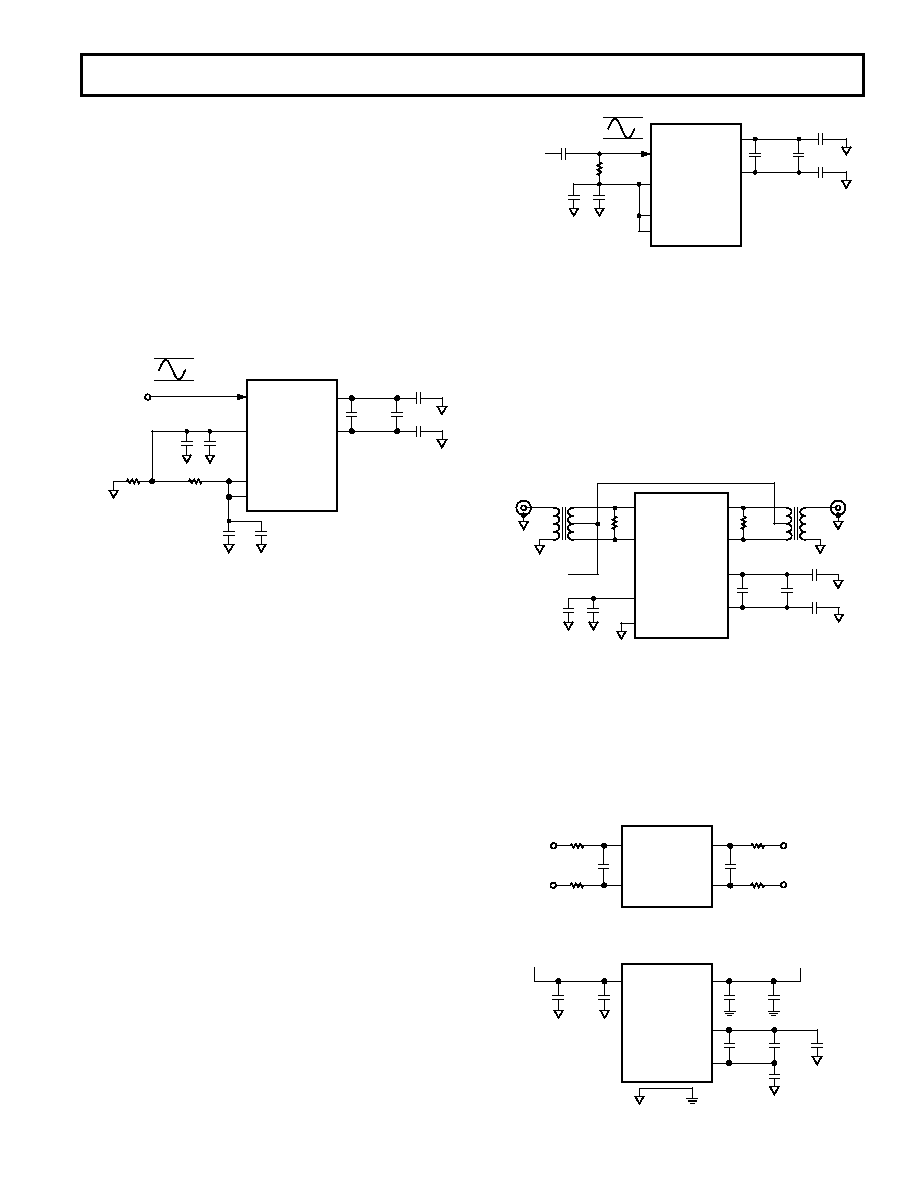
EXAMPLE: For a single-ended input range from 0 V to 1 V
applied to IINA, we would configure the converter for a 1 V
reference (see Figure 17) and apply 0.5 V to IINB.
I OR QREFT
I OR QREFB
IINA
IINB
VREF
REF SENSE
0.1 F
10 F
0.1 F
AD9281
0.1 F
10 F
MIDSCALE
VOLTAGE
= 0.5V (1V)
1V
0V
INPUT
5k
Figure 17. Example Configuration for 0 V–1 V Single-
Ended Input Signal
Note that since the inputs are high impedance, this reference
level can easily be generated with an external resistive divider
with large resistance values (to minimize power dissipation). A
decoupling capacitor is recommended on this input to minimize
the high frequency noise-coupling onto this pin. Decoupling
should occur close to the ADC.
Differential Inputs
Use of differential input signals can provide greater flexibility in
input ranges and bias points, as well as offering improvements in
distortion performance, particularly for high frequency input
signals. Users with differential input signals will probably want
to take advantage of the differential input structure of the AD9281.
Performance is still very good for single-ended inputs. Convert-
ing a single-ended input to a differential signal for application to
the converter is probably only worth considering for very high
frequency input signals.
AC-Coupled Inputs
If the signal of interest has no dc component, ac coupling can be
easily used to define an optimum bias point. Figure 18 illustrates
one recommended configuration. The voltage chosen for the dc
bias point (in this case the 1 V reference) is applied to both
IINA and IINB pins through 1 k
resistors (R1 and R2). IINA
is coupled to the input signal through Capacitor C1, while IINB is
decoupled to ground through Capacitor C2.
0.1 F
10 F
0.1 F
ANALOG
INPUT
1.0 F
0.1 F
1k
1.5V
0.5V
I OR QREFT
I OR QREFB
IINA
IINB
VREF
AD9281
REFSENSE
Figure 18. Example Configuration for 0.5 V–1.5 V ac
Coupled Single-Ended Inputs
Transformer Coupled Inputs
Another option for input ac coupling is to use a transformer.
This not only provides dc rejection, but also allows truly differ-
ential drive of the AD9281’s analog inputs, which will provide
the optimal distortion performance. Figure 19 shows a recom-
mended transformer input drive configuration. Resistors R1 and
R2 define the termination impedance of the transformer cou-
pling. The center tap of the transformer secondary is tied to the
common-mode voltage, establishing the dc bias point for the
analog inputs.
0.1 F10 F
0.1 F
COMMON
MODE
VOLTAGE
0.1 F
10 F
R1
R2
I OR QREFT
I OR QREFB
IINA
IINB
AD9281
QINB
QINA
REFSENSE
VREF
Figure 19. Example Configuration for Transformer
Coupled Inputs
Crosstalk:
The internal layout of the AD9281, as well as its
pinout, was configured to minimize the crosstalk between the
two input signals. Users wishing to minimize high frequency
crosstalk should take care to provide the best possible decoupling
for input pins (see Figure 20). R and C values will make a pole
dependant on antialiasing requirements. Decoupling is also
required on reference pins and power supplies (see Figure 21).
QINA
QINB
IINA
IINB
AD9281
Figure 20. Input Loading
DVDD
I OR QREFT
I OR QREFB
AVDD
0.1 F
10 F
0.1 F10 F
AD9281
0.1 F
10 F
V ANALOG
V DIGITAL
Figure 21. Reference and Power Supply Decoupling
REV. F
相关PDF资料 |
PDF描述 |
|---|---|
| AD8564ARZ-REEL7 | IC COMPARATOR QUAD 7NS 16SOIC TR |
| AD8561AR | IC COMPARATOR SNGL 7NS 8-SOIC |
| AD7274BUJZ-500RL7 | IC ADC 12BIT 3MSPS TSOT23-8 |
| VI-22Y-IV-B1 | CONVERTER MOD DC/DC 3.3V 99W |
| VI-201-IX-B1 | CONVERTER MOD DC/DC 12V 75W |
相关代理商/技术参数 |
参数描述 |
|---|---|
| AD9281ARSZ | 制造商:Analog Devices 功能描述:IC 8BIT ADC SMD 9281 SOIC28 |
| AD9281ARSZRL | 功能描述:IC ADC 8BIT DUAL CMOS 28SSOP RoHS:是 类别:集成电路 (IC) >> 数据采集 - 模数转换器 系列:- 标准包装:1,000 系列:- 位数:16 采样率(每秒):45k 数据接口:串行 转换器数目:2 功率耗散(最大):315mW 电压电源:模拟和数字 工作温度:0°C ~ 70°C 安装类型:表面贴装 封装/外壳:28-SOIC(0.295",7.50mm 宽) 供应商设备封装:28-SOIC W 包装:带卷 (TR) 输入数目和类型:2 个单端,单极 |
| AD9281-EB | 制造商:Analog Devices 功能描述:DEV TOOLS, EVAL BD FOR AD9281 - Bulk |
| AD9283 | 制造商:AD 制造商全称:Analog Devices 功能描述:8-Bit, 50 MSPS/80 MSPS/100 MSPS 3 V A/D Converter |
| AD9283/PCB | 制造商:Analog Devices 功能描述:8 BIT 100 MSPS 3.3V A/D CONVERTER - Bulk |
发布紧急采购,3分钟左右您将得到回复。