- 您现在的位置:买卖IC网 > PDF目录10681 > AD9281ARSZ (Analog Devices Inc)IC ADC 8BIT DUAL CMOS 28-SSOP PDF资料下载
参数资料
| 型号: | AD9281ARSZ |
| 厂商: | Analog Devices Inc |
| 文件页数: | 5/15页 |
| 文件大小: | 0K |
| 描述: | IC ADC 8BIT DUAL CMOS 28-SSOP |
| 产品培训模块: | ADC Applications ADC Architectures ADC DC/AC Performance |
| 标准包装: | 47 |
| 位数: | 8 |
| 采样率(每秒): | 28M |
| 数据接口: | 并联 |
| 转换器数目: | 2 |
| 功率耗散(最大): | 260mW |
| 电压电源: | 模拟和数字 |
| 工作温度: | -40°C ~ 85°C |
| 安装类型: | 表面贴装 |
| 封装/外壳: | 28-SSOP(0.209",5.30mm 宽) |
| 供应商设备封装: | 28-SSOP |
| 包装: | 管件 |
| 输入数目和类型: | 4 个单端,单极;2 个差分,单极 |
| 产品目录页面: | 780 (CN2011-ZH PDF) |
AD9281
–13–
ANALOG
CIRCUITS
DIGITAL
LOGIC
ICs
V
A
D
DVSS
AVSS
A
B
IA
ID
AVDD
DVDD
LOGIC
SUPPLY
D
A
VIN
CSTRAY
GND
A = ANALOG
D = DIGITAL
ADC
IC
DIGITAL
CIRCUITS
A
Figure 31. Ground and Power Consideration
These characteristics result in both a reduction of electro-
magnetic interference (EMI) and an overall improvement in
performance.
It is important to design a layout that prevents noise from cou-
pling onto the input signal. Digital signals should not be run in
parallel with the input signal traces and should be routed
away from the input circuitry. Separate analog and digital
grounds should be joined together directly under the AD9281 in
a solid ground plane. The power and ground return currents
must be carefully managed. A general rule of thumb for mixed
signal layouts dictates that the return currents from digital cir-
cuitry should not pass through critical analog circuitry.
Transients between AVSS and DVSS will seriously degrade
performance of the ADC.
If the user cannot tie analog ground and digital ground together
at the ADC, he should consider the configuration in Figure 32.
Another input and ground technique is shown in Figure 32. A
separate ground plane has been split for RF or hard to manage
signals. These signals can be routed to the ADC differentially or
single ended (i.e., both can either be connected to the driver or
RF ground). The ADC will perform well with several hundred
mV of noise or signals between the RF and ADC analog ground.
DATA
ANALOG
GROUND
DIGITAL
GROUND
LOGIC
ADC
AIN
BIN
RF
GROUND
Figure 32. RF Ground Scheme
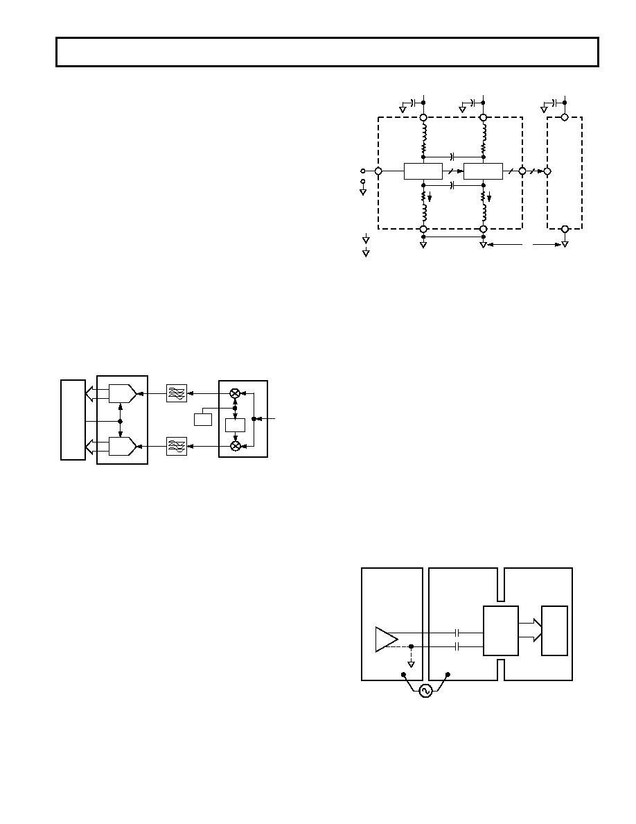
At the receiver, the demodulation of a QAM signal back into its
separate I and Q components is essentially the modulation
process explain above but in the reverse order. A common and
traditional implementation of a QAM demodulator is shown in
Figure 30. In this example, the demodulation is performed in
the analog domain using a dual, matched ADC and a quadra-
ture demodulator to recover and digitize the I and Q baseband
signals. The quadrature demodulator is typically a single IC
containing two mixers and the appropriate circuitry to generate
the necessary 90
° phase shift between the I and Q mixers’ local
oscillators. Before being digitized by the ADCs, the mixed
down baseband I and Q signals are filtered using matched ana-
log filters. These filters, often referred to as Nyquist or Pulse-
Shaping filters, remove images-from the mixing process and any
out-of-band. The characteristics of the matching Nyquist filters
are well defined to provide optimum signal-to-noise (SNR)
performance while minimizing intersymbol interference. The
ADC’s are typically simultaneously sampling their respective
inputs at the QAM symbol rate or, most often, at a multiple of it
if a digital filter follows the ADC. Oversampling and the use of
digital filtering eases the implementation and complexity of the
analog filter. It also allows for enhanced digital processing for
both carrier and symbol recovery and tuning purposes. The use
of a dual ADC such as the AD9281 ensures excellent gain,
offset, and phase matching between the I and Q channels.
90°C
FROM
PREVIOUS
STAGE
QUADRATURE
DEMODULATOR
LO
I
ADC
DSP
OR
ASIC
CARRIER
FREQUENCY
NYQUIST
FILTERS
Q
ADC
DUAL MATCHED
ADC
Figure 30. Typical Analog QAM Demodulator
GROUNDING AND LAYOUT RULES
As is the case for any high performance device, proper ground-
ing and layout techniques are essential in achieving optimal
performance. The analog and digital grounds on the AD9281
have been separated to optimize the management of return
currents in a system. Grounds should be connected near the
ADC. It is recommended that a printed circuit board (PCB) of
at least four layers, employing a ground plane and power planes,
be used with the AD9281. The use of ground and power planes
offers distinct advantages:
1. The minimization of the loop area encompassed by a signal
and its return path.
2. The minimization of the impedance associated with ground
and power paths.
3. The inherent distributed capacitor formed by the power plane,
PCB insulation and ground plane.
REV. F
相关PDF资料 |
PDF描述 |
|---|---|
| AD8564ARZ-REEL7 | IC COMPARATOR QUAD 7NS 16SOIC TR |
| AD8561AR | IC COMPARATOR SNGL 7NS 8-SOIC |
| AD7274BUJZ-500RL7 | IC ADC 12BIT 3MSPS TSOT23-8 |
| VI-22Y-IV-B1 | CONVERTER MOD DC/DC 3.3V 99W |
| VI-201-IX-B1 | CONVERTER MOD DC/DC 12V 75W |
相关代理商/技术参数 |
参数描述 |
|---|---|
| AD9281ARSZ | 制造商:Analog Devices 功能描述:IC 8BIT ADC SMD 9281 SOIC28 |
| AD9281ARSZRL | 功能描述:IC ADC 8BIT DUAL CMOS 28SSOP RoHS:是 类别:集成电路 (IC) >> 数据采集 - 模数转换器 系列:- 标准包装:1,000 系列:- 位数:16 采样率(每秒):45k 数据接口:串行 转换器数目:2 功率耗散(最大):315mW 电压电源:模拟和数字 工作温度:0°C ~ 70°C 安装类型:表面贴装 封装/外壳:28-SOIC(0.295",7.50mm 宽) 供应商设备封装:28-SOIC W 包装:带卷 (TR) 输入数目和类型:2 个单端,单极 |
| AD9281-EB | 制造商:Analog Devices 功能描述:DEV TOOLS, EVAL BD FOR AD9281 - Bulk |
| AD9283 | 制造商:AD 制造商全称:Analog Devices 功能描述:8-Bit, 50 MSPS/80 MSPS/100 MSPS 3 V A/D Converter |
| AD9283/PCB | 制造商:Analog Devices 功能描述:8 BIT 100 MSPS 3.3V A/D CONVERTER - Bulk |
发布紧急采购,3分钟左右您将得到回复。